13192EVB-BDM-A0E Freescale Semiconductor, 13192EVB-BDM-A0E Datasheet - Page 18
13192EVB-BDM-A0E
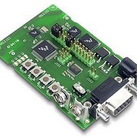
Manufacturer Part Number
13192EVB-BDM-A0E
Description
EVAL BOARD HARDWARE DEV
Manufacturer
Freescale Semiconductor
Type
802.15.4/Zigbeer
Specifications of 13192EVB-BDM-A0E
Contents
Hardware, Software, Documentation and USB Multilink
Wireless Frequency
2.4 GHz
Interface Type
SPI
Modulation
DSSS OQPSK
Security
128 bit AES
Operating Voltage
2 VDC to 3.4 VDC
Output Power
1 mW
Operating Temperature Range
- 40 C to + 85 C
For Use With/related Products
MC13193
Lead Free Status / RoHS Status
Lead free / RoHS Compliant


Applications Information
Since the MC13192 contains an on-chip reference frequency trim capability, it is possible to trim out
virtually all of the initial tolerance factors and put the frequency within 0.12 ppm on a board-by-board
basis.
A tolerance analysis budget may be created using all the previously stated factors. It is an engineering
judgment whether the worst case tolerance will assume that all factors will vary in the same direction or if
the various factors can be statistically rationalized using RSS (Root-Sum-Square) analysis. The aging
factor is usually specified in ppm/year and the product designer can determine how many years are to be
assumed for the product lifetime. Taking all of the factors into account, the product designer can determine
the needed specifications for the crystal and external load capacitors to meet the 802.15.4 Standard.
8.2
Design Example
Figure 11
shows a basic application schematic for interfacing the MC13192 with an MCU.
Table 9
lists
the Bill of Materials (BOM).
The MC13192 has differential RF inputs and outputs that are well suited to balanced printed wire antenna
structures. Alternatively, as in the application circuit, a printed wire antenna, a chip antenna, or other
single-ended structures can be used with commercially available chip baluns or microstrip equivalents.
PAO+ and PAO- require a DC connection to VDDA (the analog regulator output) through AC blocking
elements. This is accomplished through the baluns in the referenced design.
The 16 MHz crystal should be mounted close to the MC13192 because the crystal trim default assumes
that the listed KDS Daishinku crystal (see
Table
10) and the 6.8 pF load capacitors shown are used. If a
different crystal is used, it should have a specified load capacitance (stray capacitance, etc.) of
9 pF or less. Other crystals are listed in
Section 8.3, “Crystal
Requirements.
VDDA is an analog regulator output used to supply only the onboard PA (PAO+ and PAO-) and VDDLO1
and VDDLO2 pins. VDDA should not be used to power devices external to the transceiver chip. Bypassing
capacitors are critical and should be placed close to the device. Unused pins should be grounded as shown.
The SPI connections to the MCU include CE, MOSI, MISO, and SPICLK. The SPI can run at a frequency
of 8 MHz or less. Optionally, CLKO can provide a clock to the MCU. The CLKO frequency is
programmable via the SPI and has a default of 32.786+ kHz (16 MHz / 488). The ATTN line can be driven
by a GPIO from the MCU (as shown) or can also be controlled by a switch or other hardware. The latter
approach allows the MCU to be put into a sleep mode and then awakened by CLKO when the ATTN line
wakes up the MC13192. RXTXEN is used to initiate receive, transmit or CCA/ED sequences under MCU
control. RXTXEN must be controlled by an MCU GPIO with the connection shown. Device reset (RST)
is controlled through a connection to an MCU GPIO.
When the MC13192 is used in Stream Mode, as with 802.15.4 MAC/PHY software, the MC13192 GPIO1
functions as an “Out of Idle” indicator and GPIO2 functions as a “CRC Valid” / Clear Channel Assessment
(CCA) result indicator and are not available for general purpose use.
MC13192 Technical Data, Rev. 3.3
18
Freescale Semiconductor
Related parts for 13192EVB-BDM-A0E
Image
Part Number
Description
Manufacturer
Datasheet
Request
R

Part Number:
Description:
EVAL BOARD HARDWARE DEV
Manufacturer:
Freescale Semiconductor
Datasheet:

Part Number:
Description:
Manufacturer:
Freescale Semiconductor, Inc
Datasheet:
Part Number:
Description:
Manufacturer:
Freescale Semiconductor, Inc
Datasheet:
Part Number:
Description:
Manufacturer:
Freescale Semiconductor, Inc
Datasheet:
Part Number:
Description:
Manufacturer:
Freescale Semiconductor, Inc
Datasheet:
Part Number:
Description:
Manufacturer:
Freescale Semiconductor, Inc
Datasheet:
Part Number:
Description:
Manufacturer:
Freescale Semiconductor, Inc
Datasheet:
Part Number:
Description:
Manufacturer:
Freescale Semiconductor, Inc
Datasheet:
Part Number:
Description:
Manufacturer:
Freescale Semiconductor, Inc
Datasheet:
Part Number:
Description:
Manufacturer:
Freescale Semiconductor, Inc
Datasheet:
Part Number:
Description:
Manufacturer:
Freescale Semiconductor, Inc
Datasheet:
Part Number:
Description:
Manufacturer:
Freescale Semiconductor, Inc
Datasheet:
Part Number:
Description:
Manufacturer:
Freescale Semiconductor, Inc
Datasheet:
Part Number:
Description:
Manufacturer:
Freescale Semiconductor, Inc
Datasheet:
Part Number:
Description:
Manufacturer:
Freescale Semiconductor, Inc
Datasheet: