BGA6589,135 NXP Semiconductors, BGA6589,135 Datasheet
BGA6589,135
Specifications of BGA6589,135
934057503135
BGA6589


Related parts for BGA6589,135


BGA6589,135 Summary of contents
Page 1
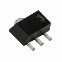
BGA6589 MMIC wideband medium power amplifier Rev. 02 — 25 May 2009 1. Product profile 1.1 General description The BGA6589 is a silicon Monolithic Microwave Integrated Circuit (MMIC) wideband medium power amplifier with internal matching circuit in a 3-pin SOT89 ...
Page 2
... NXP Semiconductors 1.4 Quick reference data Table 1. Symbol L1dB 2. Pinning information Table 2. Pin Ordering information Table 3. Type number BGA6589 4. Marking Table 4. Type number BGA6589 BGA6589_2 Product data sheet Quick reference data Parameter DC device voltage DC supply current insertion power gain noise figure ...
Page 3
... NXP Semiconductors 5. Limiting values Table 5. In accordance with the Absolute Maximum Rating System (IEC 60134). Symbol tot T stg [ Thermal characteristics Table 6. Symbol R th(j-sp) [ Characteristics Table Symbol Parameter [ operating supply voltage applied Table (see Figure Symbol Parameter LIN R LOUT BGA6589_2 Product data sheet ...
Page 4
... NXP Semiconductors Table (see Figure Symbol Parameter L1dB IP3 (in) IP3 (out) Fig 1. BGA6589_2 Product data sheet Characteristics …continued = 81 mA IP3 S amb bias 10 unless otherwise specified noise figure stability factor load power gain compression input intercept point output intercept point 135 ...
Page 5
... NXP Semiconductors Fig (dB 500 1000 1500 mA dBm Fig 3. Insertion gain ( function of 21 frequency; typical values BGA6589_2 Product data sheet 135 0.5 0.2 2.6 GHz 0 0.2 0.5 180 0.2 0.5 135 mA dBm Output reflection coefficient (s 22 mgx412 |s 12 (dB) 2000 2500 f (MHz ...
Page 6
... NXP Semiconductors 25 P L1dB (dBm 500 1000 1500 mA Fig 5. Load power as a function of frequency; typical values 500 1000 1500 mA Fig 7. Stability factor as a function of frequency; typical values BGA6589_2 Product data sheet mgx413 40 IP3 (out) (dBm 2000 2500 0 f (MHz Fig 6. Output intercept as a function of frequency; ...
Page 7
... NXP Semiconductors Fig 9. 8. Application information Figure 10 internally matched and therefore does not require any external matching. The value of the input and output DC blocking capacitors C1 and C2 depends on the operating frequency; see fine tune the input and output impedance. Capacitor supply decoupling capacitor. ...
Page 8
... NXP Semiconductors Table 9. List of components See Figure 10 for circuit. Component Description C1, C2 multilayer ceramic chip capacitor C3 multilayer ceramic chip capacitor C4 multilayer ceramic chip capacitor [1] C5 electrolytic or tantalum capacitor L1 SMD inductor R1 SMD resistor, 0 [1] Optional. Table 10. Scattering parameters mA dBm (MHz Magnitude Angle ...
Page 9
... NXP Semiconductors Table 10. Scattering parameters mA dBm (MHz Magnitude Angle (ratio) (degree) 2500 0.22 132.8 2600 0.21 141.3 2700 0.21 153.3 2800 0.07 127.7 2900 0.19 167.20 3000 0.18 178.11 3100 0.18 165.13 BGA6589_2 Product data sheet …continued = amb Magnitude Angle Magnitude ...
Page 10
... NXP Semiconductors 9. Package outline Plastic surface-mounted package; collector pad for good heat transfer; 3 leads DIMENSIONS (mm are the original dimensions) UNIT 1.6 0.48 0.53 1.8 mm 1.4 0.35 0.40 1.4 OUTLINE VERSION IEC SOT89 Fig 11. Package outline SOT89 (SC-62) BGA6589_2 Product data sheet ...
Page 11
... Document ID Release date BGA6589_2 20090525 • Modifications: The format of this data sheet has been redesigned to comply with the new identity guidelines of NXP Semiconductors. • Legal texts have been adapted to the new company name where appropriate. • Changed I • Table 1: changed symbol V • ...
Page 12
... Right to make changes — NXP Semiconductors reserves the right to make changes to information published in this document, including without limitation specifications and product descriptions, at any time and without notice ...
Page 13
... NXP Semiconductors 14. Contents 1 Product profi 1.1 General description 1.2 Features . . . . . . . . . . . . . . . . . . . . . . . . . . . . . . 1 1.3 Applications . . . . . . . . . . . . . . . . . . . . . . . . . . . 1 1.4 Quick reference data Pinning information . . . . . . . . . . . . . . . . . . . . . . 2 3 Ordering information . . . . . . . . . . . . . . . . . . . . . 2 4 Marking . . . . . . . . . . . . . . . . . . . . . . . . . . . . . . . . 2 5 Limiting values Thermal characteristics Characteristics . . . . . . . . . . . . . . . . . . . . . . . . . . 3 8 Application information Package outline . . . . . . . . . . . . . . . . . . . . . . . . 10 10 Abbreviations . . . . . . . . . . . . . . . . . . . . . . . . . . 11 11 Revision history . . . . . . . . . . . . . . . . . . . . . . . . 11 12 Legal information ...