SI4735-B20-GM Silicon Laboratories Inc, SI4735-B20-GM Datasheet - Page 12
SI4735-B20-GM
Manufacturer Part Number
SI4735-B20-GM
Description
IC RX AM/FM/SW/LW RAD RDS 20UQFN
Manufacturer
Silicon Laboratories Inc
Datasheet
1.SI4735-B-EVB.pdf
(24 pages)
Specifications of SI4735-B20-GM
Package / Case
20-UQFN, 20-µQFN
Frequency
153kHz ~ 279kHz, 520kHz ~ 1.71MHz, 2.3MHz ~ 21.85MHz, 64MHz ~ 108MHz
Modulation Or Protocol
AM, FM, LW-SW, WB
Applications
General Purpose
Current - Receiving
19.9mA
Data Interface
PCB, Surface Mount
Antenna Connector
PCB, Surface Mount
Features
RSSI Equipped
Voltage - Supply
2.7 V ~ 5.5 V
Operating Temperature
-20°C ~ 85°C
Bus Type
I2C
Maximum Frequency
108 MHz, 1710 MHz
Minimum Frequency
76 MHz, 520 MHz
Modulation Technique
AM, FM
Mounting Style
SMD/SMT
Function
Radio
Supply Voltage (min)
2.7 V
Supply Voltage (max)
5.5 V
Minimum Operating Temperature
- 20 C
Maximum Operating Temperature
+ 85 C
Lead Free Status / RoHS Status
Lead free / RoHS Compliant
Sensitivity
-
Memory Size
-
Data Rate - Maximum
-
Lead Free Status / Rohs Status
Compliant
Available stocks
Company
Part Number
Manufacturer
Quantity
Price
Company:

Part Number:
SI4735-B20-GM
Manufacturer:
SiliconL
Quantity:
85
Part Number:
SI4735-B20-GMR
Manufacturer:
SILICON LABS/芯科
Quantity:
20 000


Si473x-B20
Table 7. FM Receiver Characteristics
(V
12
Parameter
Seek/Tune Time
Powerup Time
RSSI Offset
Notes:
DD
1. Additional testing information is available in “AN388: Si470x/1x/2x/3x/4x Evaluation Test Board Procedure.”
2. To ensure proper operation and receiver performance, follow the guidelines in “AN383: Si47xx Antenna, Schematic,
3. F
4. f = 22.5 kHz.
5. B
6. Guaranteed by characterization.
7. V
8. |f
9. f = 75 kHz.
10. At L
11. Analog audio output mode.
12. At temperature (25°C).
= 2.7 to 5.5 V, V
Volume = maximum for all tests. Tested at RF = 98.1 MHz.
Layout and Design Guidelines.” Silicon Laboratories will evaluate schematics and layouts for qualified customers.
2
MOD
AF
EMF
– f
OUT
= 300 Hz to 15 kHz, A-weighted.
1
12
= 1 mV.
= 1 kHz, 75
| > 2 MHz,
and R
6
6
IO
OUT
= 1.5 to 3.6 V, T
f
0
µ
pins.
s de-emphasis, MONO = enabled, and L = R unless noted otherwise.
= 2 x f
1
– f
2
A
. AGC
= –20 to 85 °C)
Symbol
1,2
is disabled.
(Continued)
60 dBµV at RF Input
Input levels of 8 and
From powerdown
RCLK tolerance
Test Condition
Rev. 0.5
= 100 ppm
Min
–3
—
—
Typ
—
—
—
Max
110
80
3
ms/channel
Unit
ms
dB
Related parts for SI4735-B20-GM
Image
Part Number
Description
Manufacturer
Datasheet
Request
R

Part Number:
Description:
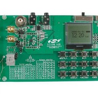
BOARD EVAL SI4735 VERSION B
Manufacturer:
Silicon Laboratories Inc
Datasheet:

Part Number:
Description:
BOARD EVAL SI4735 VERSION C
Manufacturer:
Silicon Laboratories Inc
Datasheet:
Part Number:
Description:
IC RX AM/FM/SW/LW RAD RDS 20UQFN
Manufacturer:
Silicon Laboratories Inc
Datasheet:
Part Number:
Description:
IC RX AM/FM/SW/LW RAD RDS 20UQFN
Manufacturer:
Silicon Laboratories Inc
Datasheet:
Part Number:
Description:
IC RX AM/FM/SW/LW RAD RDS 20UQFN
Manufacturer:
Silicon Laboratories Inc
Datasheet:
Part Number:
Description:
IC RX AM/FM/SW/LW RAD RDS 24SSOP
Manufacturer:
Silicon Laboratories Inc
Datasheet:
Part Number:
Description:
BOARD EVALUATION FOR SI4734/35
Manufacturer:
Silicon Laboratories Inc
Datasheet:
Part Number:
Description:
RF RX FM AM SW LW 24 SSOP
Manufacturer:
Silicon Laboratories Inc
Datasheet:
Part Number:
Description:
IC RAD RX AM/FM/SW/LW/AUX 20QFN
Manufacturer:
Silicon Laboratories Inc
Datasheet:
Part Number:
Description:
IC RX AM/FM/SW/LW RAD RDS 24SSOP
Manufacturer:
Silicon Laboratories Inc
Datasheet:
Part Number:
Description:
RECEIVER, RADIO, MULTIBAND, 20QFN
Manufacturer:
Silicon Laboratories Inc
Datasheet:
Part Number:
Description:
SMD/C�/SINGLE-ENDED OUTPUT SILICON OSCILLATOR
Manufacturer:
Silicon Laboratories Inc
Part Number:
Description:
Manufacturer:
Silicon Laboratories Inc
Datasheet:
Part Number:
Description:
N/A N/A/SI4010 AES KEYFOB DEMO WITH LCD RX
Manufacturer:
Silicon Laboratories Inc
Datasheet: