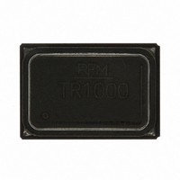
TR1000 RFM, TR1000 Datasheet - Page 5

TR1000
Manufacturer Part Number
TR1000
Description
ASH TR 115.2 KBPS 916.5 MHZ
Manufacturer
RFM
Series
TRr
Datasheet
1.TR1000.pdf
(12 pages)
Specifications of TR1000
Frequency
916.5MHz
Data Rate - Maximum
115.2kbps
Modulation Or Protocol
ASK, OOK
Applications
General Data Transfer
Sensitivity
-106dBm
Voltage - Supply
2.2 V ~ 3.7 V
Current - Receiving
3.8mA
Current - Transmitting
1.5mA
Data Interface
PCB, Surface Mount
Antenna Connector
PCB, Surface Mount
Operating Temperature
-40°C ~ 85°C
Package / Case
SM-20H
Wireless Frequency
916.5 MHz
Output Power
1.5 dBm
Operating Supply Voltage
2.5 V, 3.3 V
Maximum Operating Temperature
+ 85 C
Mounting Style
SMD/SMT
Maximum Data Rate
115.2 Kbps
Minimum Operating Temperature
- 40 C
Modulation
OOK/ASK
Lead Free Status / RoHS Status
Lead free by exemption / RoHS compliant by exemption
Power - Output
-
Memory Size
-
Lead Free Status / Rohs Status
Lead free / RoHS Compliant
Other names
583-1088-2
Available stocks
Company
Part Number
Manufacturer
Quantity
Price
Company:
Part Number:
TR1000-LRIP
Manufacturer:
HRS
Quantity:
159
www.RFM.com
©2008 by RF Monolithics, Inc.
Figure 2
Since an amplifier-sequenced receiver is inherently a sampling
receiver, the overall cycle time between the start of one RFA1 ON
sequence and the start of the next RFA1 ON sequence should be
set to sample the narrowest RF data pulse at least 10 times.
Otherwise, significant edge jitter will be added to the detected data
pulse.
ASH Transceiver Block Diagram
Figure 2 is the general block diagram of the ASH transceiver.
Please refer to Figure 2 for the following discussions.
Antenna Port
The only external RF components needed for the transceiver are
the antenna and its matching components. Antennas presenting
an impedance in the range of 35 to 72 ohms resistive can be
satisfactorily matched to the RFIO pin with a series matching coil
and a shunt matching/ESD protection coil. Other antenna
impedances can be matched using two or three components. For
some impedances, two inductors and a capacitor will be required.
A DC path from RFIO to ground is required for ESD protection.
Receiver Chain
The output of the SAW filter drives amplifier RFA1. This amplifier
includes provisions for detecting the onset of saturation (AGC Set),
and for switching between 35 dB of gain and 5 dB of gain (Gain
Select). AGC Set is an input to the AGC Control function, and Gain
Select is the AGC Control function output. ON/OFF control to
RFA1 (and RFA2) is generated by the Pulse Generator & RF Amp
Bias function. The output of RFA1 drives the SAW delay line, which
has a nominal delay of 0.5 µs.
The second amplifier, RFA2, provides 51 dB of gain below
saturation. The output of RFA2 drives a full-wave detector with
Tuning/ESD
Antenna
Tuning
RFIO
20
CR Filter
E-mail: info@rfm.com
SAW
TXMOD
RFA1
TXA2
TX
IN
PRATE
& Bias Control
Modulation
R
8
TXM
TRL1
CN
Pulse Generator
& RF Amp Bias
17
14
Gain Select
R
Delay Line
AGC Set
PR
TRL0
SAW
CN
TXA1
18
15
PWIDTH
R
PW
ASH Transceiver Block Diagram
Power Down
Control
RFA2
AGCCAP
Log
Detector
Control
AGC
VCC1: Pin 2
VCC2: Pin 16
GND1: Pin 1
GND2: Pin 10
GND3: Pin 19
RREF: Pin 11
CMPIN: Pin 6
3
C
AGC
LPFADJ
Low-Pass
Filter
19 dB of threshold gain. The onset of saturation in each section of
RFA2 is detected and summed to provide a logarithmic response.
This is added to the output of the full-wave detector to produce an
overall detector response that is square law for low signal levels,
and transitions into a log response for high signal levels. This
combination provides excellent threshold sensitivity and more than
70 dB of detector dynamic range. In combination with the 30 dB of
AGC range in RFA1, more than 100 dB of receiver dynamic range
is achieved.
The detector output drives a gyrator filter. The filter provides a
three-pole, 0.05 degree equiripple low-pass response with
excellent group delay flatness and minimal pulse ringing. The 3 dB
bandwidth of the filter can be set from 4.5 kHz to 1.8 MHz with an
external resistor.
The filter is followed by a base-band amplifier which boosts the
detected signal to the BBOUT pin. When the receiver RF amplifiers
are operating at a 50%-50% duty cycle, the BBOUT signal
changes about 10 mV/dB, with a peak-to-peak signal level of up to
685 mV. For lower duty cycles, the mV/dB slope and peak-to-peak
signal level are proportionately less. The detected signal is riding
on a 1.1 Vdc level that varies somewhat with supply voltage,
temperature, etc. BBOUT is coupled to the CMPIN pin or to an
external data recovery process (DSP, etc.) by a series capacitor.
The correct value of the series capacitor depends on data rate,
data run length, and other factors as discussed in the ASH
Transceiver Designer’s Guide.
When an external data recovery process is used with AGC,
BBOUT must be coupled to the external data recovery process
and CMPIN by separate series coupling capacitors. The AGC
reset function is driven by the signal applied to CMPIN.
9
R
AGC Reset
LPF
BB
5
C
BBO
6
BBOUT
PKDET
Detector
Peak
AGC
4
THLD1
C
PKD
Ref
13
Ref
R
Threshold
TH1
Control
DS2
DS1
11
dB Below
Peak Thld
R
Thld
REF
R
TH2
12
THLD2
AND
7
TR1000 - 4/4/08
RXDATA
Page 5 of 12


