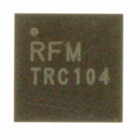
TRC104 RFM, TRC104 Datasheet - Page 13

TRC104
Manufacturer Part Number
TRC104
Description
IC TXRX RF 2.4GHZ MULTICHAN
Manufacturer
RFM
Datasheet
1.DR-TRC104-2400-DK.pdf
(33 pages)
Specifications of TRC104
Frequency
2.4GHz Center
Data Rate - Maximum
1Mbps
Modulation Or Protocol
GFSK
Applications
Automotive Systems, Consumer Systems
Sensitivity
-95dBm
Voltage - Supply
1.9 V ~ 3.6 V
Current - Receiving
18mA
Current - Transmitting
13mA
Data Interface
PCB, Surface Mount
Antenna Connector
PCB, Surface Mount
Operating Temperature
-40°C ~ 85°C
Package / Case
24-LLP
Wireless Frequency
2.4 GHz
Operating Supply Voltage
2.5 V, 3.3 V
Maximum Operating Temperature
+ 85 C
Mounting Style
SMD/SMT
Minimum Operating Temperature
- 40 C
Modulation
GFSK
Lead Free Status / RoHS Status
Lead free / RoHS Compliant
Power - Output
-
Memory Size
-
Lead Free Status / Rohs Status
Lead free / RoHS Compliant
Other names
583-1136-2
Figure 9
4.2 Stop Mode
In Stop Mode the contents of the TRC104 configuration registers are maintained, and the digital voltage regulator
and parts of the digital circuitry are enabled. The remaining digital and analog circuitry is disabled to minimize
current consumption, which is typically 1.4 µA. No serial transaction can occur in Stop Mode. The typical turn-on
time from Stop Mode is 1.5 ms. Any operation to the TRC104 must wait until the turn on period is complete.
Figure 10 demonstrates the states of the mode control pins and the timing related to Stop Mode.
Figure 10
4.3 Standby Mode
Stand-by Mode is a low current mode that provides a very low transition time to configuration, transmit or receive
modes. In Standby Mode circuit blocks that are not being utilized are shutdown to minimize current usage. When
the TRC104 is set to Transmit, Receive or Configuration Mode, there is no start-up delay and the next action may
occur immediately. The power consumption of Standby Mode is dictated mainly by the crystal frequency used.
4.4 Configuration Mode
Configuration Mode allows access to the TRC104’s configuration registers. Serial data is applied to the SDAT pin
and serial clock is applied to the SCLK pin. See Section 5 for additional details.
4.5 Transmit/Receive Mode
This mode is enabled to load the transmit FIFO or receive data. The mode function, transmit or receive, is set
before enabling this mode. The mode function is selected by the C_Mode bit in configuration register 0x00. See
Section 5 for descriptions and timing of the various data transfer modes.
www.RFM.com
E-mail:
info@rfm.com
Technical support +1.800.704.6079
Page 13 of 33
©2009 by RF Monolithics, Inc.
TRC104 - 08/13/09


