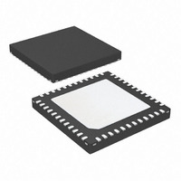
ATA5824-PLQW Atmel, ATA5824-PLQW Datasheet - Page 32

ATA5824-PLQW
Manufacturer Part Number
ATA5824-PLQW
Description
IC TXRX UHF ASK/FSK 48QFN
Manufacturer
Atmel
Datasheet
1.ATA5824-PLQW.pdf
(98 pages)
Specifications of ATA5824-PLQW
Frequency
433 ~ 435MHz; 866 ~ 870MHz
Data Rate - Maximum
20kbps
Modulation Or Protocol
ASK, FSK
Applications
RKE, TPM, Security Systems
Power - Output
10dBm
Sensitivity
-116dBm
Voltage - Supply
2.15 V ~ 3.6 V or 4.4 V ~ 5.25 V
Current - Receiving
10.5mA
Current - Transmitting
10.5mA
Data Interface
PCB, Surface Mount
Antenna Connector
PCB, Surface Mount
Operating Temperature
-40°C ~ 105°C
Package / Case
48-VQFN Exposed Pad, 48-HVQFN, 48-SQFN, 48-DHVQFN
Lead Free Status / RoHS Status
Lead free / RoHS Compliant
Memory Size
-
Available stocks
Company
Part Number
Manufacturer
Quantity
Price
Company:
Part Number:
ATA5824-PLQW
Manufacturer:
ATMEL
Quantity:
3 500
Part Number:
ATA5824-PLQW
Manufacturer:
ATMEL/爱特梅尔
Quantity:
20 000
32
ATA5823/ATA5824
The supply voltage range of the ATA5823/ATA5824 is 2.15V to 3.6V or 4.4V to 5.25V.
Pin VS1 is the supply voltage input for the range 2.15V to 3.6V and is used in battery applica-
tions using a single lithium 3V cell. Pin VS2 is the voltage input for the range 4.4V to 5.25V (car
applications), in this case the voltage regulator V_REG regulates VS1 to typically 3.25V. If the
voltage regulator is active, a blocking capacitor of 2.2 µF has to be connected to VS1.
Pin VSINT is the voltage input for the Microcontroller_Interface and must be connected to the
power supply of the microcontroller. The voltage range of V
10-5
AVCC is the internal operation voltage of the RF transceiver and is feed via the switch
SW_AVCC by VS1. AVCC must be blocked on pin AVCC with a 68 nF capacitor (see
on page
DVCC is the internal operation voltage of the digital control logic and is fed via the switch
SW_DVCC by VS1. DVCC must be blocked on pin DVCC with 68 nF (see
Figure 4-1 on page
Pin PWR_ON is an input to switch on the transceiver (active high).
Pin N_PWR_ON is an input for a push button and can also be used to switch on the transceiver
(active low).
For current consumption reasons it is recommended to set N_PWR_ON to GND only tempo-
rarily. Otherwise an additional current flows because of a 50 k pull-up resistor.
A voltage monitor generates the signal DVCC_OK if DVCC
Figure 10-2. Flow Chart Operation Modes
and
AVCC = VS1; DVCC = VS1
6,
Figure 10-6 on page
Figure 4-1 on page
TX Mode
OPM2 OPM1 OPM0
7,
0
0
0
1
1
Figure 5-1 on page 8
OFF command and
Pin PWR_ON = 0 and
Pin N_ PWR_ON = 1
0
1
1
0
1
RX Polling
1
0
1
1
1
Mode
35).
7,
TX mode
RX polling mode
RX mode
FD mode (maaster)
FD mode (slave)
Figure 5-1 on page 8
Pin PWR_ON = 1 or
Pin N_ PWR_ON = 0
AVCC = OFF
DVCC = OFF
AVCC = VS1
DVCC = VS1
IDLE Mode
and
OFF Mode
RX Mode
Figure 6-1 on page
and
Figure 6-1 on page
FD Mode
VSINT
(Slave)
1.6V typically.
is 2.25V to 5.25V (see
9).
Figure 3-1 on page
FD Mode
(Master)
9).
4829D–RKE–06/06
Figure 3-1
Figure
6,


