ATA5824-PLQW Atmel, ATA5824-PLQW Datasheet - Page 80
ATA5824-PLQW
Manufacturer Part Number
ATA5824-PLQW
Description
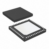
IC TXRX UHF ASK/FSK 48QFN
Manufacturer
Atmel
Datasheet
1.ATA5824-PLQW.pdf
(98 pages)
Specifications of ATA5824-PLQW
Frequency
433 ~ 435MHz; 866 ~ 870MHz
Data Rate - Maximum
20kbps
Modulation Or Protocol
ASK, FSK
Applications
RKE, TPM, Security Systems
Power - Output
10dBm
Sensitivity
-116dBm
Voltage - Supply
2.15 V ~ 3.6 V or 4.4 V ~ 5.25 V
Current - Receiving
10.5mA
Current - Transmitting
10.5mA
Data Interface
PCB, Surface Mount
Antenna Connector
PCB, Surface Mount
Operating Temperature
-40°C ~ 105°C
Package / Case
48-VQFN Exposed Pad, 48-HVQFN, 48-SQFN, 48-DHVQFN
Lead Free Status / RoHS Status
Lead free / RoHS Compliant
Memory Size
-
Available stocks
Company
Part Number
Manufacturer
Quantity
Price
Company:

Part Number:
ATA5824-PLQW
Manufacturer:
ATMEL
Quantity:
3 500
Part Number:
ATA5824-PLQW
Manufacturer:
ATMEL/爱特梅尔
Quantity:
20 000


17. Electrical Characteristics: General (Continued)
All parameters refer to GND and are valid for T
V
f
can be found in the specific sections of the “Electrical Characteristics”.
80
*) Type means: A = 100% tested, B = 100% correlation tested, C = Characterized on samples, D = Design parameter
Note:
RF
4.10 Output Power FD2
VS2
No. Parameters
4.4
4.5
4.6
4.7 Output Power FD1
4.8
4.9
= 433.92 MHz (battery application) unless otherwise specified. Details about current consumption, timing and digital pin properties
= 4.4V to 5.6V, V
Supply current
FD mode 4
Input sensitivity FD
mode
Sensitivity change
FD mode
Output Power FD1
variation for full
temperature range
Output Power FD1
variation for full
temperature and supply
voltage range
1. Pin numbers in brackets mean they were measured with RF_IN matched to 50 according to
ATA5823/ATA5824
component values according to
page 22
VSINT
with component values according to
= 4.4V to 5.25V (car application). Typical values are given at V
Test Conditions
P
R
PWSET=31
Load optimized for
+5 dBm!
V
T
PER = 5%
P(RF
–30 dBm
–35 dBm
–40 dBm
–45 dBm
–50 dBm
Bit rate 5 Kbit/s
V
Coupling Phase 0° to 360°
T
Frequency offset max.
±50 kHz
S = S
V
T
R
PWSET = 13
Load optimized for
+5 dBm!
V
T
R
PWSET = 13
P = P
V
T
R
PWSET = 13
P = P
V
T
R
PWSET = 20
Load optimized for
+5 dBm!
amb
amb
amb
amb
amb
amb
out
VS1
VS1
VS1
VS1
VS1
VS1
R_PWR
R_PWR
R_PWR
R_PWR
R_PWR
= 5 dBm
= V
= 25°C,
= V
= –40°C to +105°C
= V
= 25°C
= V
= –40°C to 105°C
= V
= –40°C to 105°C
= V
= 25°C
OUT
REFRX_FD
REFTX_FD1
REFTX_FD1
= 22 k
= 22 k
= 22 k
= 22 k
= 22 k
VS2
VS2
VS2
VS2
VS2
VS2
@RF
= 3 V
= 2.15V to 3.6V
= 3V
= 3V
= 2.15V to 3.6V
= 3V
Table 7-2 on page 12
IN
amb
+ S
+ P
+ P
):
= –40°C to +105°C, V
REFRX_FD
REFTX_FD1
REFTX_FD1
Table 7-7 on page 22
17,18,
Pin
(10)
(10)
(10)
(10)
27
(4)
(4)
(1)
(RF
IN
VS1
) and RF_OUT matched to 50 according to
P
P
S
P
P
S
Symbol
REFTX_FD1
REFTX_FD2
REFRX_FD
= V
REFTX_FD1
REFTX_FD1
I
REFRX_FD
S_FD4
VS2
(RF
= V
OUT
VSINT
).
–100.5
–101.5
–88.5
–93.5
–97.5
–12.5
Min.
–5.5
–7.5
VS1
–3
–3
= 2.15V to 3.6V (battery application), and
= V
VS2
= V
–100
–103
–104
Typ.
15.2
–1.5
–91
–96
–10
–5
0
VSINT
Figure 7-1 on page 11
= 3V and T
–101.5
–104.5
–105.5
–92.5
–97.5
Max.
–7.5
–2.5
2.5
5
2
Figure 7-12 on
amb
4829D–RKE–06/06
dBm
dBm
dBm
Unit
mA
dB
dB
dB
= 25°C,
Type*
with
B
B
B
B
B
B
B
Related parts for ATA5824-PLQW
Image
Part Number
Description
Manufacturer
Datasheet
Request
R

Part Number:
Description:
RF Transceiver RF Data Control Duplex Trans.
Manufacturer:
Atmel
Datasheet:

Part Number:
Description:
Manufacturer:
Atmel
Datasheet:

Part Number:
Description:
DEV KIT FOR AVR/AVR32
Manufacturer:
Atmel
Datasheet:

Part Number:
Description:
INTERVAL AND WIPE/WASH WIPER CONTROL IC WITH DELAY
Manufacturer:
ATMEL Corporation
Datasheet:
Part Number:
Description:
Low-Voltage Voice-Switched IC for Hands-Free Operation
Manufacturer:
ATMEL Corporation
Datasheet:
Part Number:
Description:
MONOLITHIC INTEGRATED FEATUREPHONE CIRCUIT
Manufacturer:
ATMEL Corporation
Datasheet:
Part Number:
Description:
AM-FM Receiver IC U4255BM-M
Manufacturer:
ATMEL Corporation
Datasheet:
Part Number:
Description:
Monolithic Integrated Feature Phone Circuit
Manufacturer:
ATMEL Corporation
Datasheet:
Part Number:
Description:
Multistandard Video-IF and Quasi Parallel Sound Processing
Manufacturer:
ATMEL Corporation
Datasheet:
Part Number:
Description:
High-performance EE PLD
Manufacturer:
ATMEL Corporation
Datasheet:
Part Number:
Description:
8-bit Flash Microcontroller
Manufacturer:
ATMEL Corporation
Datasheet:
Part Number:
Description:
2-Wire Serial EEPROM
Manufacturer:
ATMEL Corporation
Datasheet: