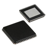
CYRF6936-40LFXC Cypress Semiconductor Corp, CYRF6936-40LFXC Datasheet - Page 6

CYRF6936-40LFXC
Manufacturer Part Number
CYRF6936-40LFXC
Description
IC WIRELESS USB LP 40VQFN
Manufacturer
Cypress Semiconductor Corp
Datasheet
1.CYRF6936-40LFXC.pdf
(23 pages)
Specifications of CYRF6936-40LFXC
Frequency
2.4GHz
Data Rate - Maximum
1Mbps
Modulation Or Protocol
DSSS, GFSK
Applications
Remote Control
Power - Output
4dBm
Sensitivity
-97dBm
Voltage - Supply
1.8 V ~ 3.6 V
Current - Receiving
21.2mA
Current - Transmitting
34mA
Data Interface
PCB, Surface Mount
Antenna Connector
PCB, Surface Mount
Operating Temperature
0°C ~ 70°C
Package / Case
40-VQFN Exposed Pad, 40-HVQFN, 40-SQFN, 40-DHVQFN
Interface
SPI
Termination Type
SMD
Bandwidth
876kHz
Supply Voltage Max
3.6V
Data Rate Max
1000Kbps
Frequency Band Type
ISM
Features
10
Frequency Band Range
2.400 - 2.483 GHz
Supply Voltage Min
2.4V
Lead Free Status / RoHS Status
Lead free / RoHS Compliant
Memory Size
-
Lead Free Status / Rohs Status
Lead free / RoHS Compliant
Other names
428-2024
CYRF6936-40LFXC
CYRF6936-40LFXC
Available stocks
Company
Part Number
Manufacturer
Quantity
Price
Company:
Part Number:
CYRF6936-40LFXC
Manufacturer:
CYPRESS
Quantity:
210
Part Number:
CYRF6936-40LFXC
Manufacturer:
CRIIUS
Quantity:
20 000
The device registers may be written to or read from one byte at
a time, or several sequential register locations may be written or
read in a single SPI transaction using incrementing burst mode.
In addition to single byte configuration registers, the device
includes register files. Register files are FIFOs written to and
read from using nonincrementing burst SPI transactions.
The IRQ pin function may be optionally multiplexed onto the
MOSI pin. When this option is enabled, the IRQ function is not
available while the SS pin is LOW. When using this configuration,
user firmware must ensure that the MOSI pin on the MCU is in a
high impedance state whenever the SS pin is HIGH.
Document #: 38-16015 Rev. *H
MOSI
MISO
MOSI
MISO
MOSI
MISO
MOSI
MISO
Bit Name
SCK
SCK
SCK
SCK
Bit #
SS
SS
SS
SS
DIR
7
DIR
DIR
DIR
DIR
0
0
1
1
cmd
cmd
cmd
cmd
INC
INC
INC
INC
A5
A5
A5
A5
INC
6
A4
A4
A4
A4
A3
A3
A3
A3
addr
addr
addr
addr
Figure 6. SPI Incrementing Burst Read Sequence
Figure 8. SPI Incrementing Burst Write Sequence
A2
A2
A2
A2
Byte 1
A1
A1
A1
A1
Figure 5. SPI Single Read Sequence
Figure 7. SPI Single Write Sequence
Figure 4. SPI Transaction Format
A0
A0
A0
A0
Address
D7
D7
D7
D7
[5:0]
D6
D6
D6
D6
D5
D5
D5
D5
data from mcu
data from mcu
data to mcu
data to mcu
D4
D4
D4
D4
The SPI interface is not dependent on the internal 12 MHz clock.
Registers may therefore be read from or written to when the
device is in sleep mode, and the 12 MHz oscillator disabled.
The SPI interface and the IRQ and RST pins have a separate
voltage reference pin (V
directly to MCUs operating at voltages below the CYRF6936 IC
supply voltage.
D3
D3
D3
D3
1
D2
D2
D2
D2
1
D1
D1
D1
D1
D0
D0
D0
D0
D7
D7
D6
D6
D5
data from mcu
D5
IO
data to mcu
). This enables the device to interface
D4
D4
Byte 1+N
D3
D3
Data
[7:0]
1+N
1+N
D2
D2
D1
D1
D0
D0
CYRF6936
Page 6 of 23
[+] Feedback


