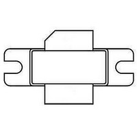
BLF7G27L-100,112 NXP Semiconductors, BLF7G27L-100,112 Datasheet - Page 3

BLF7G27L-100,112
Manufacturer Part Number
BLF7G27L-100,112
Description
TRANSISTOR PWR LDMOS SOT502
Manufacturer
NXP Semiconductors
Datasheet
1.BLF7G27L-100118.pdf
(14 pages)
Specifications of BLF7G27L-100,112
Package / Case
SOT502A
Transistor Type
LDMOS
Frequency
2.6GHz ~ 2.7GHz
Gain
17.5dB
Voltage - Rated
65V
Current - Test
900mA
Voltage - Test
28V
Mounting Style
SMD/SMT
Transistor Polarity
N-Channel
Configuration
Single
Drain-source Breakdown Voltage
65 V
Lead Free Status / RoHS Status
Lead free / RoHS Compliant
Current Rating
-
Power - Output
-
Noise Figure
-
Lead Free Status / RoHS Status
Lead free / RoHS Compliant, Lead free / RoHS Compliant
NXP Semiconductors
6. Characteristics
7. Test information
BLF7G27L-100_7G27LS-100
Preliminary data sheet
7.1 Ruggedness in class-AB operation
Table 6.
T
Remark: All testing performed in a class-AB production test circuit.
Table 7.
Mode of operation: 1-carrier N-CDMA, single carrier IS-95 with pilot, paging, sync and 6 traffic
channels (Walsh codes 8 - 13). PAR = 9.7 dB at 0.01 % probability on the CCDF, channel bandwidth
is 1.2288 MHz; f
T
The BLF7G27L-100 and BLF7G27LS-100 are capable of withstanding a load mismatch
corresponding to VSWR = 10 : 1 through all phases under the following conditions:
V
Symbol Parameter
V
V
I
I
I
g
R
Symbol
P
G
RL
η
ACPR
DSS
DSX
GSS
j
case
DS
fs
D
(BR)DSS
GS(th)
L(AV)
DS(on)
p
= 25
in
= 28 V; I
= 25
885k
°
C unless otherwise specified.
°
drain-source breakdown voltage
gate-source threshold voltage
drain leakage current
drain cut-off current
gate leakage current
forward transconductance
drain-source on-state resistance
C; unless otherwise specified.
Characteristics
Functional test information
Parameter
average output power
power gain
input return loss
drain efficiency
adjacent channel power ratio (885 kHz)
Dq
1
= 900 mA; P
All information provided in this document is subject to legal disclaimers.
= 2500 MHz; f
BLF7G27L-100; BLF7G27LS-100
Rev. 2 — 5 April 2011
L
2
= 100 W (CW); f = 2500 MHz.
= 2700 MHz; RF performance at V
Conditions
V
V
V
V
V
V
V
V
I
D
GS
DS
GS
GS
DS
GS
DS
GS
= 5.35 A
= 10 V; I
= 10 V
= 10 V; I
= 0 V; I
= 0 V; V
= V
= 11 V; V
= V
GS(th)
GS(th)
Conditions
D
DS
D
D
= 1 mA
+ 3.75 V;
+ 3.75 V;
DS
= 153 mA
= 153 mA
= 28 V
= 0 V
DS
Power LDMOS transistor
= 28 V; I
Min
65
1.5
-
25.1 29
-
-
-
Min Typ Max Unit
-
16.3 18
-
24
-
© NXP B.V. 2011. All rights reserved.
Dq
Typ
-
1.8
-
-
1.34 -
0.1
20
−10 -
28
−45 −40
= 900 mA;
-
-
-
Max Unit
-
2.3
5
-
500
-
3 of 14
W
dB
dB
%
dBc
V
V
μA
A
nA
S
Ω


