BLF7G27LS-100,112 NXP Semiconductors, BLF7G27LS-100,112 Datasheet
BLF7G27LS-100,112
Specifications of BLF7G27LS-100,112


Related parts for BLF7G27LS-100,112


BLF7G27LS-100,112 Summary of contents
Page 1
... BLF7G27L-100; BLF7G27LS-100 Power LDMOS transistor Rev. 2 — 5 April 2011 1. Product profile 1.1 General description 100 W LDMOS power transistor for base station applications at frequencies from 2500 MHz to 2700 MHz. Table 1. Typical RF performance at T Mode of operation IS-95 Single carrier W-CDMA 2500 to 2700 900 [1] Single carrier IS-95 with pilot, paging, sync and 6 traffic channels (Walsh codes 8 - 13) ...
Page 2
... NXP Semiconductors 2. Pinning information Table 2. Pin BLF7G27L-100 (SOT502A BLF7G27LS-100 (SOT502B [1] Connected to flange. 3. Ordering information Table 3. Type number BLF7G27L-100 BLF7G27LS-100 4. Limiting values Table 4. In accordance with the Absolute Maximum Rating System (IEC 60134). Symbol stg Thermal characteristics Table 5. Symbol Parameter R th(j-c) BLF7G27L-100_7G27LS-100 Preliminary data sheet BLF7G27L-100 ...
Page 3
... P L(AV η D ACPR 885k 7.1 Ruggedness in class-AB operation The BLF7G27L-100 and BLF7G27LS-100 are capable of withstanding a load mismatch corresponding to VSWR = through all phases under the following conditions BLF7G27L-100_7G27LS-100 Preliminary data sheet BLF7G27L-100; BLF7G27LS-100 Characteristics C unless otherwise specified. drain-source breakdown voltage gate-source threshold voltage ...
Page 4
... 900 mA ( 2500 MHz ( 2600 MHz ( 2700 MHz Fig 1. Single carrier IS-95 power gain as a function of average output power; typical values BLF7G27L-100_7G27LS-100 Preliminary data sheet BLF7G27L-100; BLF7G27LS-100 001aan538 η D (%) (3) (2) ( (W) L(AV) ( 2500 MHz ( 2600 MHz ( 2700 MHz Fig 2. All information provided in this document is subject to legal disclaimers. ...
Page 5
... 900 mA ( 2500 MHz ( 2600 MHz ( 2700 MHz Fig 5. Single carrier IS-95 peak-to-average power ratio as a function of average output power; typical values BLF7G27L-100_7G27LS-100 Preliminary data sheet BLF7G27L-100; BLF7G27LS-100 001aan540 −50 ACPR 1980k (dBc) −60 (1) (2) (3) −70 − (W) L(AV) ( 2500 MHz ( 2600 MHz ( 2700 MHz Fig 4 ...
Page 6
... 900 mA ( 2500 MHz ( 2600 MHz ( 2700 MHz Fig 7. Pulsed CW power gain as a function of output power; typical values BLF7G27L-100_7G27LS-100 Preliminary data sheet BLF7G27L-100; BLF7G27LS-100 001aan544 (1) (2) (3) 80 120 P (W) L Fig 8. All information provided in this document is subject to legal disclaimers. Rev. 2 — 5 April 2011 ...
Page 7
... 900 mA ( 2500 MHz ( 2600 MHz ( 2700 MHz Fig 9. Single carrier W-CDMA power gain as a function of average output power; typical values BLF7G27L-100_7G27LS-100 Preliminary data sheet BLF7G27L-100; BLF7G27LS-100 001aan546 η D (%) (W) L(AV) ( 2500 MHz ( 2600 MHz ( 2700 MHz Fig 10. Single carrier W-CDMA drain efficiency as a All information provided in this document is subject to legal disclaimers. Rev. 2 — ...
Page 8
... 900 mA ( 2500 MHz ( 2600 MHz ( 2700 MHz Fig 13. Single carrier W-CDMA peak-to-average power ratio as a function of average output power; typical values BLF7G27L-100_7G27LS-100 Preliminary data sheet BLF7G27L-100; BLF7G27LS-100 001aan548 −50 ACPR (dBc) −60 (1) (2) (3) −70 − (W) L(AV) ( 2500 MHz ( 2600 MHz ( 2700 MHz Fig 12 ...
Page 9
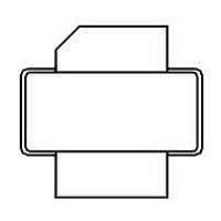
... UNIT 12.83 4.72 0.15 20.02 mm 12.57 3.43 0.08 19.61 0.505 0.186 0.006 0.788 inches 0.135 0.495 0.772 0.003 OUTLINE VERSION IEC SOT502A Fig 15. Package outline SOT502A BLF7G27L-100_7G27LS-100 Preliminary data sheet BLF7G27L-100; BLF7G27LS-100 scale 19.96 9.50 9.53 1.14 19.94 5.33 19.66 9.30 9 ...
Page 10
... DIMENSIONS (millimetre dimensions are derived from the original inch dimensions) c UNIT 12.83 4.72 0.15 20.02 mm 12.57 3.43 0.08 19.61 0.505 0.186 0.006 0.788 inches 0.135 0.495 0.772 0.003 OUTLINE VERSION IEC SOT502B Fig 16. Package outline SOT502B BLF7G27L-100_7G27LS-100 Preliminary data sheet BLF7G27L-100; BLF7G27LS-100 scale 19.96 9.50 9.53 1.14 19.94 5.33 19.66 9 ...
Page 11
... Revision history Table 9. Revision history Document ID BLF7G27L-100_7G27LS-100 v.2 20110405 Modifications: BLF7G27L-100_7G27LS-100 v.1 20100421 BLF7G27L-100_7G27LS-100 Preliminary data sheet BLF7G27L-100; BLF7G27LS-100 Abbreviations Description Complementary Cumulative Distribution Function Continuous Wave Interim Standard 95 ElectroStatic Discharge Laterally Diffused Metal Oxide Semiconductor Laterally Diffused Metal Oxide Semiconductor Transistor ...
Page 12
... BLF7G27L-100_7G27LS-100 Preliminary data sheet BLF7G27L-100; BLF7G27LS-100 [3] Definition This document contains data from the objective specification for product development. This document contains data from the preliminary specification. ...
Page 13
... For sales office addresses, please send an email to: BLF7G27L-100_7G27LS-100 Preliminary data sheet BLF7G27L-100; BLF7G27LS-100 NXP Semiconductors’ specifications such use shall be solely at customer’s own risk, and (c) customer fully indemnifies NXP Semiconductors for any liability, damages or failed product claims resulting from customer design and use of the product for automotive applications beyond NXP Semiconductors’ ...
Page 14
... Trademarks Contact information Contents . . . . . . . . . . . . . . . . . . . . . . . . . . . . . . 14 BLF7G27L-100; BLF7G27LS-100 Please be aware that important notices concerning this document and the product(s) described herein, have been included in section ‘Legal information’. © NXP B.V. 2011. For more information, please visit: http://www.nxp.com For sales office addresses, please send an email to: salesaddresses@nxp.com Power LDMOS transistor All rights reserved ...