Chameleon-AVR Nurve Networks, Chameleon-AVR Datasheet - Page 21
Chameleon-AVR
Manufacturer Part Number
Chameleon-AVR
Description
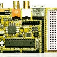
MCU, MPU & DSP Development Tools AVR8 & PROPELLER DEV SYSTEM (SBC)
Manufacturer
Nurve Networks
Datasheet
1.CHAMELEON-AVR.pdf
(268 pages)
Specifications of Chameleon-AVR
Processor To Be Evaluated
AVR 328P
Data Bus Width
8 bit
Interface Type
USB, VGA, PS/2, I2C, ISP, SPI
Operating Supply Voltage
3.3 V, 5 V
Lead Free Status / RoHS Status
Lead free / RoHS Compliant


/RESET – Reset input. A low level on this pin for longer than the minimum pulse length will generate a reset, even if the
clock is not running.
XTAL1 - Input to the inverting Oscillator amplifier and input to the internal clock operating circuit.
XTAL2 – Output from the inverting Oscillator amplifier.
VCC – Main power, 5V.
GND – System ground.
AVCC - AVCC is the supply voltage pin for the Analog-to-digital Converter. It should be externally connected to VCC,
even if the ADC is not used. If the ADC is used, it should be connected to VCC through a low-pass filter.
AREF - This is the analog reference pin for the Analog-to-digital Converter.
The AVR 328P is a 8-bit RISC-like architecture chip with instructions being either 16 or 32-bits in size (mostly 16-bit).
The memory model is a “Hardware Architecture” meaning that the data and memory are located in separate memories
that are not addressed as a contiguous space, but rather as separate memories with different instructions to read/write to
them. This allows faster execution since the same buses aren’t used to access data and program space. Therefore, you
will typically access SRAM as a continuous 2K of memory and program/FLASH memory is in a completely different
address space as is EEPROM memory. Thus, there are 3 different memories that the AVR 328P supports. Additionally,
the AVR 328P maps registers as well as all it’s I/O ports in the SRAM memory space for ease of access. Figure 1.6 show
these memories.
Referring to Figure 1.6, Program Memory is composed of both a “Boot FLASH Section” and the “Application
Section”. The boot section holds boot ROM code and can be different sizes or disabled. The application section then
holds the actual run-time code for the application. The Data Memory is stored in SRAM of course and is 2048 bytes in
length. However, due to register space allocation there is a shift in the addresses; the first 256 byte addresses are used to
access registers and system I/O then from address [$0100 - $08FF] is the 2K block of free memory. Not shown in the
TIP
Harvard as opposed to Von Neumann architecture are the two primary computer
memory organizations used in modern processors. Harvard was created at Harvard
University, thus the moniker, and likewise Von Neumann was designed by
mathematician John Von Neumann Von Neumann differs from Harvard in that Von
Neumann uses a single memory for both data and program storage.
Figure 1.6 – FLASH and SRAM memory layouts.
© 2009 NURVE NETWORKS LLC “Exploring the Chameleon AVR 8-Bit”
21
Related parts for Chameleon-AVR
Image
Part Number
Description
Manufacturer
Datasheet
Request
R

Part Number:
Description:
MCU, MPU & DSP Development Tools PIC24 & PROPELLER DEV SYSTEM (SBC)
Manufacturer:
Nurve Networks
Datasheet:

Part Number:
Description:
MCU, MPU & DSP Development Tools AVR8 VIDEO GAME DEV SYSTEM (SBC)
Manufacturer:
Nurve Networks

Part Number:
Description:
MCU, MPU & DSP Development Tools PIC24 VIDEO GAME DEV SYSTEM (SBC)
Manufacturer:
Nurve Networks