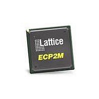
LFE2M20SE-5FN484C Lattice, LFE2M20SE-5FN484C Datasheet - Page 10

LFE2M20SE-5FN484C
Manufacturer Part Number
LFE2M20SE-5FN484C
Description
FPGA - Field Programmable Gate Array 19K LUTs 304 I/O S-Ser SERDES DSP -5
Manufacturer
Lattice
Datasheet
1.LFE2-12SE-6FN256C.pdf
(389 pages)
Specifications of LFE2M20SE-5FN484C
Number Of Macrocells
19000
Maximum Operating Frequency
311 MHz
Number Of Programmable I/os
304
Data Ram Size
1246208
Supply Voltage (max)
1.26 V
Maximum Operating Temperature
+ 85 C
Minimum Operating Temperature
0 C
Mounting Style
SMD/SMT
Supply Voltage (min)
1.14 V
Package / Case
FPBGA-484
Lead Free Status / RoHS Status
Lead free / RoHS Compliant
Available stocks
Company
Part Number
Manufacturer
Quantity
Price
Company:
Part Number:
LFE2M20SE-5FN484C
Manufacturer:
Lattice
Quantity:
135
Company:
Part Number:
LFE2M20SE-5FN484C
Manufacturer:
LATTICE
Quantity:
12
Company:
Part Number:
LFE2M20SE-5FN484C
Manufacturer:
Lattice Semiconductor Corporation
Quantity:
10 000
- Current page: 10 of 389
- Download datasheet (5Mb)
Lattice Semiconductor
Figure 2-5. General Purpose PLL (GPLL) Diagram
Standard PLL (SPLL)
Some of the larger devices have two to six Standard PLLs (SPLLs). SPLLs have the same features as GPLLs but
without delay adjustment capability. SPLLs also provide different parametric specifications. For more information,
please see the list of additional technical documentation at the end of this data sheet.
Table 2-4 provides a description of the signals in the GPLL and SPLL blocks.
Table 2-4. GPLL and SPLL Blocks Signal Descriptions
CLKI
CLKFB
RST
RSTK
CLKOS
CLKOP
CLKOK
LOCK
DDAMODE
DDAIZR
DDAILAG
DDAIDEL[2:0]
DPA MODES
DPHASE [3:0]
DDDUTY [3:0]
1. These signals are not available in SPLL.
from clock net(CLKOP) or from
(from routing or external pin)
from CLKOP (PLL internal),
a user clock (pin or logic)
Signal
1
1
1
1
CLKI
CLKFB
RST
RSTK
I/O
—
O
O
O
O
I
I
I
I
I
I
I
I
I
I
Input Clock
Feedback
(CLKFB)
Divider
Divider
(CLKI)
Clock input from external pin or routing
Dynamic Delay Enable. “1”: Pin control (dynamic), “0”: Fuse Control (static)
Dynamic Delay Zero. “1”: delay = 0, “0”: delay = on
Dynamic Delay Lag/Lead. “1”: Lead, “0”: Lag
DPA (Dynamic Phase Adjust/Duty Cycle Select) mode
DPA Phase Adjust inputs
DPA Duty Cycle Select inputs
PLL feedback input from CLKOP (PLL internal), from clock net (CLKOP) or from a user clock
(PIN or logic)
“1” to reset PLL counters, VCO, charge pumps and M-dividers
“1” to reset K-divider
PLL output clock to clock tree (phase shifted/duty cycle changed)
PLL output clock to clock tree (no phase shift)
PLL output to clock tree through secondary clock divider
“1” indicates PLL LOCK to CLKI
Dynamic Delay Input
Dynamic Delay Adjustment
Adjust
Delay
2-7
Controlled
Oscillator
Voltage
(Optional External Capacitor)
PLLCAP External Pin
Description
Post Scalar
(CLKOP)
LatticeECP2/M Family Data Sheet
Divider
Dynamic Adjustment
Phase/Duty
Secondary
(CLKOK)
Divider
Select
Architecture
CLKOK
CLKOP
CLKOS
LOCK
Related parts for LFE2M20SE-5FN484C
Image
Part Number
Description
Manufacturer
Datasheet
Request
R

Part Number:
Description:
FPGA - Field Programmable Gate Array 19K LUTs 140 I/O S-Ser SERDES DSP -5
Manufacturer:
Lattice
Datasheet:
Part Number:
Description:
FPGA LatticeECP2M Family 19000 Cells 90nm (CMOS) Technology 1.2V 484-Pin FBGA
Manufacturer:
LATTICE SEMICONDUCTOR
Datasheet:

Part Number:
Description:
FPGA LatticeECP2M Family 19000 Cells 90nm (CMOS) Technology 1.2V 256-Pin FBGA
Manufacturer:
Lattice
Datasheet:

Part Number:
Description:
IC FPGA 20KLUTS 140I/O 256-BGA
Manufacturer:
Lattice
Datasheet:

Part Number:
Description:
IC FPGA 20KLUTS 140I/O 256-BGA
Manufacturer:
Lattice
Datasheet:

Part Number:
Description:
IC FPGA 20KLUTS 304I/O 484-BGA
Manufacturer:
Lattice
Datasheet:

Part Number:
Description:
IC FPGA 19KLUTS 484FGPBGA
Manufacturer:
Lattice
Datasheet:

Part Number:
Description:
FPGA - Field Programmable Gate Array 19K LUTs 304 I/O S-Ser SERD DSP -6
Manufacturer:
Lattice

Part Number:
Description:
FPGA - Field Programmable Gate Array 19K LUTs 304 I/O S-Ser SERD DSP -7
Manufacturer:
Lattice

Part Number:
Description:
FPGA - Field Programmable Gate Array 19K LUTs 140 I/O S-Ser SERD DSP -6 I
Manufacturer:
Lattice

Part Number:
Description:
FPGA - Field Programmable Gate Array 19K LUTs 140 I/O S-Ser SERD DSP -6
Manufacturer:
Lattice

Part Number:
Description:
FPGA - Field Programmable Gate Array 19K LUTs 304 I/O S-Ser SERDES DSP -5
Manufacturer:
Lattice

Part Number:
Description:
FPGA - Field Programmable Gate Array 19K LUTs 304 I/O S-Ser SERD DSP -6 I
Manufacturer:
Lattice


