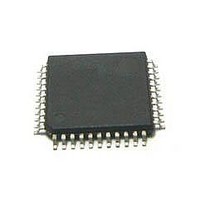
MC56F8255VLD Freescale Semiconductor, MC56F8255VLD Datasheet - Page 29

MC56F8255VLD
Manufacturer Part Number
MC56F8255VLD
Description
DSC 64K FLASH 60MHZ 44-LQFP
Manufacturer
Freescale Semiconductor
Series
56F8xxxr
Datasheets
1.TWR-56F8257.pdf
(88 pages)
2.MC56F8245VLD.pdf
(14 pages)
3.MC56F8245VLD.pdf
(2 pages)
4.MC56F8245VLD.pdf
(629 pages)
Specifications of MC56F8255VLD
Core Processor
56800E
Core Size
16-Bit
Speed
60MHz
Connectivity
CAN, I²C, LIN, SCI, SPI
Peripherals
LVD, POR, PWM, WDT
Number Of I /o
35
Program Memory Size
64KB (32K x 16)
Program Memory Type
FLASH
Ram Size
4K x 16
Voltage - Supply (vcc/vdd)
3 V ~ 3.6 V
Data Converters
A/D 8x12b, D/A 1x12b
Oscillator Type
Internal
Operating Temperature
-40°C ~ 105°C
Package / Case
44-LQFP
Product
DSCs
Processor Series
56800E
Core
56800E
Device Million Instructions Per Second
60 MIPs
Maximum Clock Frequency
60 MHz
Number Of Programmable I/os
35
Data Ram Size
8 KB
Operating Supply Voltage
3.3 V
Maximum Operating Temperature
+ 105 C
Mounting Style
SMD/SMT
Minimum Operating Temperature
- 40 C
On-chip Adc
12 bit, 4 Channel
Lead Free Status / RoHS Status
Lead free / RoHS Compliant
Eeprom Size
-
Lead Free Status / Rohs Status
Details
Available stocks
Company
Part Number
Manufacturer
Quantity
Price
Company:
Part Number:
MC56F8255VLD
Manufacturer:
Freescale Semiconductor
Quantity:
10 000
1
4
4.1
The MC56F825x/MC56F824x device is based on the 56800E core. It uses a dual Harvard-style architecture with two
independent memory spaces for data and program. On-chip RAM is shared by both data and program spaces; flash memory is
used only in program space.
This section provides memory maps for:
On-chip memory sizes for the device are summarized in
Restrictions” column of
Freescale Semiconductor
(PWM3X)
GPIOF6
GPIOF7
GPIOF8
(RXD0)
Signal
Name
(TB2)
(TB3)
(TB1)
•
•
If CLKIN is selected as the device’s external clock input, both the GPS_C0 bit in GPS1 and the EXT_SEL bit in the OCCS
oscillator control register (OSCTL) must be set. In this case, it is also recommended to power down the crystal oscillator.
Program address space, including the interrupt vector table
Data address space, including the EOnCE memory and peripheral memory maps
Memory Maps
Introduction
LQFP
44
Table 5. MC56F825x/MC56F824x Signal and Package Information (continued)
LQFP
48
Table
LQFP
64
58
59
6
6.
MC56F825x/MC56F824x Digital Signal Controller, Rev. 3
Output
Output
Output
Output
Output
Output
Output
Input/
Input/
Input/
Input/
Input/
Input/
Input/
Type
Input
enabled
enabled
enabled
internal
internal
internal
During
Reset
pullup
pullup
pullup
Input,
Input,
Input,
State
Table
Port F GPIO — This GPIO pin can be individually programmed as
an input or output pin.
TB2 — Quad timer module B channel 2 input/output.
PWM3X — Enhanced PWM submodule 3 output X or input capture
X
After reset, the default state is GPIOF6.
Port F GPIO — This GPIO pin can be individually programmed as
an input or output pin.
TB3 — Quad timer module B channel 3 input/output.
After reset, the default state is GPIOF7.
Port F GPIO — This GPIO pin can be individually programmed as
an input or output pin.
RXD0 — The SCI0 receive data input.
TB1 — Quad timer module B channel 1 input/output.
After reset, the default state is GPIOF8.
6. Flash memories’ restrictions are identified in the “Use
Signal Description
Memory Maps
29


