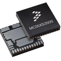
MC35XS3500PNA Freescale Semiconductor, MC35XS3500PNA Datasheet - Page 34

MC35XS3500PNA
Manufacturer Part Number
MC35XS3500PNA
Description
IC SWITCH HIGHSIDE 24PQFN
Manufacturer
Freescale Semiconductor
Type
High Side Switchr
Datasheet
1.MC35XS3500PNAR2.pdf
(41 pages)
Specifications of MC35XS3500PNA
Number Of Outputs
5
Rds (on)
*
Internal Switch(s)
Yes
Current Limit
9A
Voltage - Input
7 V ~ 20 V
Operating Temperature
-40°C ~ 125°C
Mounting Type
Surface Mount
Package / Case
24-PQFN, 24-PowerQFN
Product
MOSFET Gate Drivers
Rise Time
50 ns
Fall Time
50 ns
Propagation Delay Time
6.5 ms
Supply Voltage (max)
+ 5.5 V
Supply Voltage (min)
- 0.3 V
Supply Current
20 mA
Maximum Operating Temperature
+ 125
Minimum Operating Temperature
- 40 C
Lead Free Status / RoHS Status
Lead free / RoHS Compliant
Available stocks
Company
Part Number
Manufacturer
Quantity
Price
WD Bit D10
ISO 7637), the VCC line is still operating, while the VBAT line
is negative. Without loads on OUT1:5 terminal, an external
clamp between V
exceeding maximum rating. The maximum external clamp
voltage shall be between the reverse battery condition and
-20 V.
without load on OUT outputs.
Loss of Supply Lines
line. The detection of the supply line failure is provided inside
the device itself.
Loss of VBAT
(V
(wake=1), the outputs [1-5] are switched off immediately. No
current path exists from V
(OUT6) can be controlled by the SPI if V
above to V
To delatch the fault, the under-voltage condition should be
removed and:
behavior depends on V
34
35XS350
FUNCTIONAL DEVICE OPERATION
LOGIC COMMANDS AND REGISTERS
BATPOR1
In case of negative transients on the V
Therefore, the device is protected against latch-up with or
The 35XS3500 is protected against the loss of any supply
During an under-voltage of V
• the bit D7 must be rewritten to a logic [1] in Normal
• if the device was in Fail mode, the fault will be delatched
In case of V
• all latched faults are reset if V
• all latched faults are maintained under V
mode. Application of the OCHI window depends on
toggling or not toggling the D7 bit. When the fault is
delatched, the 35XS3500 returns to the configuration it
was just before the failure.
periodically by the Autorestart feature.
conditions. In case V
outputs are OFF. OUT6 output state depends on the
previous SPI configuration. The SPI configuration,
reporting, and daisy-chain features are provided for
RST is set to logic [1] . The SPI pull-up and pull-down
current resistors are available. This fault condition can
be diagnosed with UVF fault in OD13 reporting bit. The
previous device configuration is maintained. No current
is conducted from V
CCUV
<V
BAT
0
BAT
. The fault is reported to the UVF bit (OD13).
BAT
<V
<V
BATUV
BATPOR1
and GND is mandatory to avoid
CC
75ms window watchdog
BAT
CC
:
) and with an active device
BAT
to V
to V
(Power OFF state), the
is disconnected, OUT[1:5]
BAT
BAT
CC
CC
. The external MOSFET
.
< V
CC
BAT
CCUV
remains and is
CC
line (per
,
Figure 18. Watchdog window
in nominal
1
timeout
75ms window watchdog
Loss of V
35XS3500 is switched automatically into Fail mode (no
deglich time). The external SMART MOSFET is OFF. All SPI
registers are reset and must be reprogrammed when V
goes above V
VBAT < V
LOSS OF V
not within specification: (V
register contents are reset with default values corresponding
to all SPI bits are set to logic [0] and all latched faults are also
reset.
Loss of Ground (GND)
loads (the outputs (1:5) are switched OFF), but is not
destroyed by the operating condition. Current limit resistors in
the digital input lines protect the digital supply against
excessive current (1kohm typical). The state of the external
smart power switch controlled by FETOUT is not guaranteed,
and the state of the external smart MOS is defined with an
external termination resistor.
Fatal Mistreatment of Logic I / O Pins
by a signal plausibility check according to
than 10ms typical, the 35XS3500 is switched into Fail mode.
In case of a (PWM) Clock failure, no PWM feature is
provided, and the bit D7 defines the outputs state. In case of
a SPI failure, the 35XS3500 is switched into Fail mode
(Figure
During loss a of V
If the external V
During a loss of ground, the 35XS3500 cannot operate the
The digital I / Os are protected against fatal mistreatment
In case the LIMP input is set to a logic [1] for a delay longer
.
SPI (MOSI, SCLK,
18)
(PWM) CLOCK
Input / Output
BATPOR2
Table 16. Logic I / O Plausibility Check
CC
LIMP
CC
CCUV
(Digital Logic Supply Line)
AND VBAT
BAT
.
. The device will transit in OFF mode if
CC
CS)
and V
Analog Integrated Circuit Device Data
(V
CC
CC
CC
< V
and V
Fail Mode activation
supplies are disconnected (or
CCUV
WD, D10 bit internal toggle
Signal Check Strategy
Freescale Semiconductor
BAT
0
Debounce for 10 ms
) and with wake=1, the
Frequency range
(bandpass filter)
) < V
D10 is toggled after
the window watchdog
Table
BATPOR1
16.
), all SPI
CC


