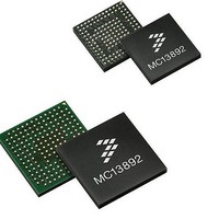
MC13892VK Freescale Semiconductor, MC13892VK Datasheet - Page 34

MC13892VK
Manufacturer Part Number
MC13892VK
Description
IC PMU I.MX51/37/35/27 139MAPBGA
Manufacturer
Freescale Semiconductor
Datasheets
1.MC13892AJVLR2.pdf
(156 pages)
2.MC13892AJVLR2.pdf
(2 pages)
3.MC13892AJVLR2.pdf
(16 pages)
Specifications of MC13892VK
Applications
Battery Management, Display (LED Drivers), Handheld/Mobile Devices, Power Supply
Operating Temperature
-40°C ~ 85°C
Mounting Type
Surface Mount
Package / Case
*
Output Current
65 mA
Output Voltage
1.5 V
Lead Free Status / RoHS Status
Lead free / RoHS Compliant
Current - Supply
-
Voltage - Supply
-
Lead Free Status / Rohs Status
Lead free / RoHS Compliant
Available stocks
Company
Part Number
Manufacturer
Quantity
Price
Company:
Part Number:
MC13892VK
Manufacturer:
FREESCALE
Quantity:
2 248
Company:
Part Number:
MC13892VK
Manufacturer:
Freescale Semiconductor
Quantity:
10 000
Company:
Part Number:
MC13892VKR2
Manufacturer:
Freescale Semiconductor
Quantity:
10 000
FUNCTIONAL DESCRIPTION
FUNCTIONAL PIN DESCRIPTION
SWITCHERS
SW1IN, SW2IN, SW3IN AND SW4IN
SW1FB, SW2FB, SW3FB AND SW4FB
point of each of their respective SWxOUT pin, in order to sense and maintain voltage stability.
SW1OUT
GNDSW1
SW2OUT
GNDSW2
SW3OUT
GNDSW3
SW4OUT
GNDSW4
DVS1 AND DVS2
The DVS pins may be reconfigured for Switcher Increment / Decrement (SID) mode control. When transitioning from one voltage
to another, the output voltage slope is controlled in steps of 25 mV per time step. These pins must be set high in order for the
DVS feature to be enabled for each of switchers 1 or 2, or low to disable it.
SWBSTIN
SWBSTOUT
SWBSTFB
sense the UVBUS pin instead of the SWBSTFB pin.
GNDSWBST
34
13892
Switchers 1, 2, 3, and 4 input. Connect these pins to BP to supply Switchers 1, 2, 3, and 4.
Switchers 1, 2, 3, and 4 feedback. Switchers 1, 2, 3, and 4 output voltage sense respectively. Connect these pins to the farther
Switcher 1 output. Buck switcher for processor core(s).
Ground for Switcher 1.
Switcher 2 output. Buck switcher for processor SOG, etc.
Ground for Switcher 2.
Switcher 3 output. Buck switcher for internal processor memory and peripherals.
Ground for switcher 3.
Switcher 4 output. Buck switcher for external memory and peripherals.
Ground for switcher 4.
Switcher 1 and 2 DVS input pins. Provided for pin controlled DVS on the buck switchers targeted for processor core supplies.
Switcher BST input. The 2.2 μH switcher BST inductor must be connected here.
Power supply for gate driver for the internal power NMOS that charges SWBST inductor. It must be connected to BP.
Switcher BST feedback. When SWBST is configured to supply the UVBUS pin in OTG mode the feedback will be switched to
Ground for switcher BST.
Analog Integrated Circuit Device Data
Freescale Semiconductor


