VNCLO-MB1A FTDI, Future Technology Devices International Ltd, VNCLO-MB1A Datasheet - Page 14
VNCLO-MB1A
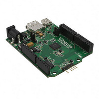
Manufacturer Part Number
VNCLO-MB1A
Description
MOD VINCULO VNC2 MOTHERBOARD
Manufacturer
FTDI, Future Technology Devices International Ltd
Series
Vinculo, Vinculum-IIr
Specifications of VNCLO-MB1A
Main Purpose
Interface, USB 2.0 Host/Controller, Arduino Shield Compatible
Embedded
Yes, MCU, 16-Bit
Utilized Ic / Part
VNC2-64Q
Primary Attributes
9V Input Power Supply, 5V Operating Voltage
Secondary Attributes
2 USB Ports
Lead Free Status / RoHS Status
Lead free / RoHS Compliant
Other names
768-1088-
768-1088-
768-1088-


4.2 Serial Peripheral Interface (SPI)
The VNC2-64Q has one master module and two slave modules. These modules are described more fully in
a
4.2.1 Signal Description - SPI Slave
The SPI Slave signals can be programmed to a choice of available I/O pins. Table 4.2 explains the
available pins for each of the SPI Slave signals. This is a subset of what the VNC2-64Q is capable of to
avoid conflict with other functions on the Vinco module.
J2-1, J2-5, J3-2, J3-5, J4-6, J5-7, J6-1,
J6-5
J2-2, J2-6, J3-1, J3-6, J4-4, J5-1, J5-4,
J5-8, J6-2, J6-6
J1-1, J2-3, J3-3, J3-7, J4-1, J4-5, J5-2,
J5-5, J6-3, J6-7
J1-2, J2-4, J3-4, J3-8, J4-2, J4-3, J5-3,
J5-6, J6-4, J6-8
Table 4.2 – Data and Control Bus Signal Mode Options – SPI Slave
Note: # defines active low signals.
4.2.2 Signal Description - SPI Master
The SPI Master signals can be programmed to a choice of available I/O pins. Table 4.3 shows the SPI
master signals and the available pins that they can be mapped.
64Q is capable of to avoid conflict with other functions on the Vinco module.
J2-1, J2-5, J3-2, J3-5, J4-6, J5-7, J6-1,
J6-5
J2-2, J2-6, J3-1, J3-6, J4-4, J5-1, J5-4,
J5-8, J6-2, J6-6
J1-1, J2-3, J3-3, J3-7, J4-1, J4-5, J5-2,
J5-5, J6-3, J6-7
J1-2, J2-4, J3-4, J3-8, J4-2, J4-3, J5-3,
J5-6, J6-4, J6-8
J2-1, J2-5, J3-2, J3-5, J4-6, J6,7, J6-1,
J6-5
Table 4.3 – Data and Control Bus Signal Mode Options – SPI Master
Note: # defines active low signals.
VNC2
datasheet please refer to: -
Available Pins
Available Pins
Copyright © 2010-2011 Future Technology Devices International Limited
FTDI website
spi_m_clk
spi_m_mosi
spi_m_miso
spi_m_ss_0#
spi_m_ss_1#
spi_s0_mosi
spi_s1_mosi
spi_s0_miso
spi_s1_miso
spi_s0_ss#
spi_s1_ss#
spi_s0_clk
spi_s1_clk
Name
Name
Vinco Development Module Datasheet Version 2.0
Input/Output
Output
Output
Output
Output
Output
Type
Input
Input
Type
Input
This is a subset of what the VNC2-
Document Reference No.: FT_000327
Active low slave select 0 from master to slave
Active low slave select 1 from master to slave
Synchronous data from master to slave
Synchronous data from slave to master
Synchronous data from master to slave
Synchronous data from slave to master
This SS# is used with the onboard ADC
Clearance No.: FTDI#173
SPI master clock input
Master Out Slave In
Master In Slave Out
(J4-6 is the default)
Master Out Slave In
(J4-4 is the default)
Master In Slave Out
(J4-5 is the default)
Slave clock input
Slave chip select
Description
Description
0
1
10
Related parts for VNCLO-MB1A
Image
Part Number
Description
Manufacturer
Datasheet
Request
R

Part Number:
Description:
POWER SUPPLY FOR VNCLO-MB1A USA
Manufacturer:
FTDI, Future Technology Devices International Ltd
Datasheet:

Part Number:
Description:
POWER SUPPLY FOR VNCLO-MB1A EU
Manufacturer:
FTDI, Future Technology Devices International Ltd
Datasheet:
Part Number:
Description:
POWER SUPPLY FOR VNCLO-MB1A UK
Manufacturer:
FTDI, Future Technology Devices International Ltd
Datasheet:

Part Number:
Description:
MOD VINCULO PIGGYBACK BOARD
Manufacturer:
FTDI, Future Technology Devices International Ltd
Datasheet:

Part Number:
Description:
MOD VINCULO W/VNC2 DEBUG MOD
Manufacturer:
FTDI, Future Technology Devices International Ltd
Datasheet:

Part Number:
Description:
IC USB TO SERIAL UART 32-QFN
Manufacturer:
FTDI, Future Technology Devices International Ltd

Part Number:
Description:
IC USB HOST CTLR VINCULUM 48LQFP
Manufacturer:
FTDI, Future Technology Devices International Ltd
Datasheet:

Part Number:
Description:
IC USB HOST VINCULUM-II 32QFN
Manufacturer:
FTDI, Future Technology Devices International Ltd
Datasheet:
Part Number:
Description:
IC USB HOST VINCULUM-II 32LQFN
Manufacturer:
FTDI, Future Technology Devices International Ltd
Datasheet:
Part Number:
Description:
IC USB HOST VINCULUM-II 48QFN
Manufacturer:
FTDI, Future Technology Devices International Ltd
Datasheet:
Part Number:
Description:
IC USB HOST VINCULUM-II 32LQFN
Manufacturer:
FTDI, Future Technology Devices International Ltd
Datasheet:
Part Number:
Description:
IC USB HOST VINCULUM-II 32QFN
Manufacturer:
FTDI, Future Technology Devices International Ltd
Datasheet:
Part Number:
Description:
IC USB HOST VINCULUM-II 48LQFP
Manufacturer:
FTDI, Future Technology Devices International Ltd
Datasheet:
Part Number:
Description:
IC USB HOST VINCULUM-II 48LQFP
Manufacturer:
FTDI, Future Technology Devices International Ltd
Datasheet:
Part Number:
Description:
IC USB HOST VINCULUM-II 48QFN
Manufacturer:
FTDI, Future Technology Devices International Ltd
Datasheet: