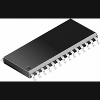
CS8420-CS Cirrus Logic Inc, CS8420-CS Datasheet - Page 27

CS8420-CS
Manufacturer Part Number
CS8420-CS
Description
Transceiver IC
Manufacturer
Cirrus Logic Inc
Datasheet
1.CS8420-CS.pdf
(80 pages)
Specifications of CS8420-CS
Audio Control Type
Sample Rate Converter
Supply Voltage Range
4.75V To 5.25V
Operating Temperature Range
-10°C To +70°C
Audio Ic Case Style
SOIC
No. Of Pins
28
Msl
MSL 2 - 1 Year
Frequency Max
108GHz
Bandwidth
20kHz
Rohs Compliant
No
Lead Free Status / RoHS Status
Contains lead / RoHS non-compliant
Available stocks
Company
Part Number
Manufacturer
Quantity
Price
Company:
Part Number:
CS8420-CS
Manufacturer:
CRY
Quantity:
5 510
Company:
Part Number:
CS8420-CS
Manufacturer:
CIRRUS
Quantity:
225
Part Number:
CS8420-CS
Manufacturer:
CRYSTAL
Quantity:
20 000
Company:
Part Number:
CS8420-CS*
Manufacturer:
NEC
Quantity:
700
Company:
Part Number:
CS8420-CSZ
Manufacturer:
CIRRUS
Quantity:
319
Company:
Part Number:
CS8420-CSZ
Manufacturer:
CIRRUS
Quantity:
9 908
Part Number:
CS8420-CSZ
Manufacturer:
CIRRUS
Quantity:
20 000
may be set or not, as desired. To begin a read, bring
CS low, send out the chip address and set the
read/write bit (R/W) high. The next falling edge of
CCLK will clock out the MSB of the addressed
register (CDOUT will leave the high impedance
state). If the MAP auto increment bit is set to 1, the
data for successive registers will appear consecu-
tively.
10.2
In I
is clocked into and out of the part by the clock,
SCL, with the clock to data relationship as shown
in Figure 25. There is no CS pin. Each individual
CS8420 is given a unique address. Pins AD0, AD1
form the 2 least significant bits of the chip address,
and should be connected to VD+ or DGND as de-
sired. The EMPH pin is used to set the AD2 bit, by
connecting a resistor from the EMPH pin to VD+
or to DGND. The state of the pin is sensed while
the CS8420 is being reset. The upper 4 bits of the
7-bit address field are fixed at 0010. To communi-
cate with a CS8420, the chip address field, which is
the first byte sent to the CS8420, should match
0010 followed by the settings of the EMPH, AD1,
and AD0. The eighth bit of the address is the R/W
bit. If the operation is a write, the next byte is the
Memory Address Pointer (MAP) which selects the
register to be read or written. If the operation is a
DS245PP2
2
C mode, SDA is a bidirectional data line. Data
I
2
C
Mode
SDA
SCL
Note 1: AD2 is derived from a resistor attached to the EMPH pin,
Note 2: If operation is a write, this byte contains the Memory Address Pointer, MAP
Start
AD1 and AD0 are determined by the state of the corresponding pins
0010
Figure 25. Control Port Timing in
AD2-0
Note 1
R/W
ACK DATA7-0 ACK DATA7-0 ACK
read, the contents of the register pointed to by the
MAP will be output. Setting the auto increment bit
in MAP allows successive reads or writes of con-
secutive registers. Each byte is separated by an ac-
knowledge bit. The ACK bit is output from the
CS8420 after each input byte is read, and is input to
the CS8420 from the microcontroller after each
transmitted byte. I
Philips Semiconductors.
10.3 Interrupts
The CS8420 has a comprehensive interrupt capa-
bility. The INT output pin is intended to drive the
interrupt input pin on the host microcontroller. The
INT pin may be set to be active low, active high or
active low with no active pull-up transistor. This
last mode is used for active low, wired-OR hook-
ups, with multiple peripherals connected to the mi-
crocontroller interrupt input pin.
Many conditions can cause an interrupt, as listed in
the interrupt status register descriptions. Each
source may be masked off via mask registers. In ad-
dition, each source may be set to rising edge, fall-
ing edge or level sensitive. Combined with the
option of level sensitive or edge sensitive modes
within the microcontroller, many different set-ups
are possible, depending on the needs of the equip-
ment designer.
Note 2
I
2
C
Mode
2
C is a registered trademark of
Stop
CS8420
27


