ADC12040CIVY National Semiconductor, ADC12040CIVY Datasheet
ADC12040CIVY
Specifications of ADC12040CIVY
Available stocks


Related parts for ADC12040CIVY

ADC12040CIVY Summary of contents
Page 1
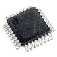
... Output data format is 12-bit offset binary. This device is available in the 32-lead LQFP package and will operate over the industrial temperature range of −40°C to +85°C. Connection Diagram © 2008 National Semiconductor Corporation Features ■ Single +5V supply operation ■ Internal sample-and-hold ■ ...
Page 2
... Ordering Information Industrial (−40°C Block Diagram www.national.com ≤ ≤ T +85°C) A ADC12040CIVY ADC12040CIVYX 32 Pin LQFP Tape and Reel ADC12040EVAL 2 Package 32 Pin LQFP Evaluation Board 20014802 ...
Page 3
Pin Descriptions and Equivalent Circuits Pin No. Symbol ANALOG I − REF DIGITAL I/O 10 CLK ...
Page 4
Pin No. Symbol ANALOG POWER AGND DIGITAL POWER DGND GND www.national.com Equivalent Circuit Positive analog supply pins. These ...
Page 5
... Absolute Maximum Ratings (Notes Military/Aerospace specified devices are required, please contact the National Semiconductor Sales Office/ Distributors for availability and specifications – Voltage on Any Input or Output Pin Input Current at Any Pin (Note 3) Package Input Current (Note 3) Package Dissipation 25°C A ESD Susceptibility ...
Page 6
Symbol Parameter REFERENCE AND ANALOG INPUT CHARACTERISTICS V Common Mode Input Voltage Input Capacitance (each pin to GND Reference Voltage (Note 13) REF Reference Input Resistance DC and Logic Electrical Characteristics Unless otherwise ...
Page 7
AC Electrical Characteristics Unless otherwise specified, the following specifications apply for AGND = DGND = DR GND = 0V 0V +2.0V MHz, t REF CLK limits 25°C (Notes ...
Page 8
Note 14 the current consumed by the switching of the output drivers and is primarily determined by load capacitance on the output pins, the supply voltage and the rate at which the outputs are switching ...
Page 9
Timing Diagram Transfer Characteristic Output Timing FIGURE 1. Transfer Characteristic 9 20014809 20014810 www.national.com ...
Page 10
Typical Performance Characteristics otherwise stated DNL DNL vs. Temperature INL www.national.com 5V 3V 20014818 DNL vs. Clock Duty Cycle 20014819 20014820 MHz MHz unless ...
Page 11
INL vs. Temperature 20014824 SNR vs. Temperature 20014828 SINAD vs. Temperature 20014825 INL vs. Clock Duty Cycle THD vs. Temperature SNR vs. Clock Duty Cycle 11 20014827 20014826 20014831 www.national.com ...
Page 12
THD vs. Clock Duty Cycle Spectral Response www.national.com SINAD and ENOB vs. Clock Duty Cycle 20014832 IMD @ F 20014829 12 20014833 = 9.5MHz 10.5MHz 1 2 20014834 ...
Page 13
Functional Description Operating on a single +5V supply, the ADC12040 uses a pipeline architecture and has error correction circuitry to help ensure maximum performance. The differential analog input signal is digitized to 12 bits. The reference input is buffered to ...
Page 14
TABLE 2. Input to Output Relationship – Single-Ended Input − V − REF CM V − REF ...
Page 15
The data in the pipeline is corrupted while in the power down mode. The Power Down Mode Exit Cycle time is determined by the value of the capacitors on pins 30, 31 ...
Page 16
FIGURE 6. Driving the Signal Inputs with a Transformer 4.0 POWER SUPPLY CONSIDERATIONS The power supply pins should be bypassed with a 10 µF ca- pacitor and with a 0.1 µF ceramic chip capacitor within a centimeter of each power ...
Page 17
To prevent this from happening, the DR GND pins should NOT be connected to system ground in close proximity to any of the ADC12040's other ground pins. Capacitive coupling ...
Page 18
Even lines with 90° crossings have capacitive coupling, so try to avoid even these 90° crossings of the clock line. FIGURE 8. Isolating the ADC Clock from other Circuitry with a Clock Tree 7.0 COMMON APPLICATION PITFALLS Driving the inputs ...
Page 19
... Physical Dimensions inches (millimeters) unless otherwise noted 32-Lead LQFP Package Ordering Number ADC12040CIVY NS Package Number VBE32A 19 www.national.com ...
Page 20
... For more National Semiconductor product information and proven design tools, visit the following Web sites at: Products Amplifiers www.national.com/amplifiers Audio www.national.com/audio Clock Conditioners www.national.com/timing Data Converters www.national.com/adc Displays www.national.com/displays Ethernet www.national.com/ethernet Interface www.national.com/interface LVDS www.national.com/lvds Power Management www.national.com/power Switching Regulators www.national.com/switchers LDOs www ...