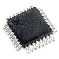
ADC12040CIVY National Semiconductor, ADC12040CIVY Datasheet - Page 6

ADC12040CIVY
Manufacturer Part Number
ADC12040CIVY
Description
IC, ADC, 12BIT, 40MSPS, LQFP-32
Manufacturer
National Semiconductor
Datasheet
1.ADC12040CIVYNOPB.pdf
(20 pages)
Specifications of ADC12040CIVY
Resolution (bits)
12bit
Sampling Rate
40MSPS
Input Channel Type
Differential
Data Interface
Parallel
Supply Voltage Range - Analog
4.75V To 5.25V
Supply Current
59mA
Digital Ic Case Style
QFP
Lead Free Status / RoHS Status
Contains lead / RoHS non-compliant
Available stocks
Company
Part Number
Manufacturer
Quantity
Price
Company:
Part Number:
ADC12040CIVY
Manufacturer:
Texas Instruments
Quantity:
10 000
Company:
Part Number:
ADC12040CIVY/NOPB
Manufacturer:
Texas Instruments
Quantity:
10 000
Company:
Part Number:
ADC12040CIVYX/NOPB
Manufacturer:
Texas Instruments
Quantity:
10 000
www.national.com
REFERENCE AND ANALOG INPUT CHARACTERISTICS
V
C
V
CLK, PD, OE DIGITAL INPUT CHARACTERISTICS
V
V
I
I
C
D0–D11 DIGITAL OUTPUT CHARACTERISTICS
V
V
I
+I
−I
POWER SUPPLY CHARACTERISTICS
I
I
I
Symbol
Symbol
IN(1)
IN(0)
OZ
A
D
DR
PSRR1 Power Supply Rejection
PSRR2 Power Supply Rejection
CM
REF
IN(1)
IN(0)
OUT(1)
OUT(0)
IN
IN
SC
SC
DC and Logic Electrical Characteristics
Unless otherwise specified, the following specifications apply for AGND = DGND = DR GND = 0V, V
PD = 0V, V
limits T
A
Logical “1” Input Voltage
Logical “0” Input Voltage
Logical “1” Input Current
Logical “0” Input Current
Digital Input Capacitance
Logical “1” Output Voltage
Logical “0” Output Voltage
TRI-STATE Output Current
Output Short Circuit Source Current
Output Short Circuit Sink Current
Analog Supply Current
Digital Supply Current
Digital Output Supply Current
Total Power Consumption
Common Mode Input Voltage
V
Reference Voltage (Note 13)
Reference Input Resistance
= T
IN
REF
Input Capacitance (each pin to GND) V
J
= 25°C (Notes 7, 8, 9)
= +2.0V, f
Parameter
Parameter
CLK
= 40 MHz, t
r
= t
f
= 3 ns, C
V
V
V
V
I
I
V
V
V
V
PD Pin = DGND, V
PD Pin = V
PD Pin = DGND
PD Pin = V
PD Pin = DGND, C
PD Pin = V
PD Pin = DGND, C
PD Pin = V
Rejection of Full-Scale Error with
V
SNR Degradation w/10 MHz,
200 mV
OUT
OUT
D
D
IN
IN
OUT
OUT
OUT
OUT
A
IN
= 5.25V
= 4.75V
= 4.75V vs. 5.25V
= 5.0V
= 0V
= 2.5 Vdc + 0.7 V
= −0.5 mA
= 1.6 mA, V
L
= 0V
= 2.5V or 5V
= 0V
= V
= 20 pF/pin. Boldface limits apply for T
P-P
DR
DR
DR
DR
DR
riding on V
, f
, f
, f
6
CLK
CLK
CLK
Conditions
Conditions
DR
REF
= 0
L
= 0
L
= 0
= 3V
= 0 pF (Note 14)
= 0 pF (Note 15)
rms
A
= 2.0V
V
V
(CLK LOW)
(CLK HIGH)
DR
DR
= 2.5V
= 3V
(Note 10)
(Note 10)
Typical
Typical
V
2.00
−100
100
−10
100
−20
340
A
10
20
59
40
58
50
A
8
7
5
8
6
0
3
0
/2
= T
A
= V
J
= T
(Note 10)
(Note 10)
D
Limits
Limits
MIN
= +5V, V
366
2.0
1.0
2.3
2.7
0.4
7.3
66
1.0
2.2
to T
MAX
DR
mA (max)
mA (max)
mA (max)
: all other
mA (min)
mA (min)
MΩ (min)
(Limits)
V (max)
V (max)
= +3.0V,
V (min)
V (min)
V (min)
(Limits)
V (max)
V (min)
Units
Units
mW
mW
mA
mA
mA
µA
µA
pF
nA
nA
dB
dB
pF
pF
V


