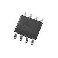
DS90LV028ATM National Semiconductor, DS90LV028ATM Datasheet - Page 3

DS90LV028ATM
Manufacturer Part Number
DS90LV028ATM
Description
IC, LVDS DIFF LINE RECEIVER, SOIC-8
Manufacturer
National Semiconductor
Datasheet
1.DS90LV028ATM.pdf
(10 pages)
Specifications of DS90LV028ATM
Supply Current
5.4mA
Supply Voltage Range
3V To 3.6V
Driver Case Style
SOIC
No. Of Pins
8
Operating Temperature Range
-40°C To +85°C
Device Type
Differential Line Receiver
Current Rating
5.4mA
Data Rate Max
400Mbps
Rohs Compliant
No
Lead Free Status / RoHS Status
Contains lead / RoHS non-compliant
Available stocks
Company
Part Number
Manufacturer
Quantity
Price
Company:
Part Number:
DS90LV028ATM
Manufacturer:
NS
Quantity:
1
Company:
Part Number:
DS90LV028ATM
Manufacturer:
NSC
Quantity:
3 005
Part Number:
DS90LV028ATM
Manufacturer:
NS/国半
Quantity:
20 000
Company:
Part Number:
DS90LV028ATM/NOPB
Manufacturer:
LT
Quantity:
32
Part Number:
DS90LV028ATMX
Manufacturer:
NS/国半
Quantity:
20 000
Note 7: Generator waveform for all tests unless otherwise specified: f = 1 MHz, Z
Note 8: t
Note 9: t
integrated circuit.
Note 10: t
and within 5˚C of each other within the operating temperature range.
Note 11: t
recommended operating temperature and voltage ranges, and across process distribution. t
Note 12: V
than 100 mV when V
Note 13: f
V
Parameter Measurement Information
Typical Application
Applications Information
General application guidelines and hints for LVDS drivers
and receivers may be found in the following application
notes: LVDS Owner’s Manual (lit #550062-002), AN-808,
AN-977, AN-971, AN-916, AN-805, AN-903.
LVDS drivers and receivers are intended to be primarily used
in an uncomplicated point-to-point configuration as is shown
in Figure 3. This configuration provides a clean signaling
OL
(max 0.4V), V
SKD1
SKD2
SKD3
MAX
SKD4
CC
is the magnitude difference in differential propagation delay time between the positive-going-edge and the negative-going-edge of the same channel.
is the differential channel-to-channel skew of any event on the same device. This specification applies to devices having multiple receivers within the
, part to part skew, is the differential channel-to-channel skew of any event between devices. This specification applies to devices at the same V
is always higher than R
generator input conditions: t
, part to part skew, is the differential channel-to-channel skew of any event between devices. This specification applies to devices over the
OH
CM
(min 2.7V), load = 15 pF (stray plus probes).
= 0V or 3V.
FIGURE 1. Receiver Propagation Delay and Transition Time Test Circuit
FIGURE 2. Receiver Propagation Delay and Transition Time Waveforms
IN
+ and R
r
= t
f
<
IN
1 ns (0% to 100%), 50% duty cycle, differential (1.05V to 1.35 peak to peak). Output criteria: 60%/40% duty cycle,
− voltage. R
FIGURE 3. Point-to-Point Application
IN
+ and R
Balanced System
IN
− are allowed to have voltage range −0.05V to +3.05V. V
3
O
= 50Ω, t
environment for the fast edge rates of the drivers. The re-
ceiver is connected to the driver through a balanced media
which may be a standard twisted pair cable, a parallel pair
cable, or simply PCB traces. Typically the characteristic
impedance of the media is in the range of 100Ω. A termina-
tion resistor of 100Ω should be selected to match the media,
and is located as close to the receiver input pins as possible.
The termination resistor converts the driver output (current
mode) into a voltage that is detected by the receiver. Other
SKD4
r
and t
is defined as |Max − Min| differential propagation delay.
f
(0% to 100%) ≤ 3 ns for R
10007703
10007705
10007704
IN
.
ID
is not allowed to be greater
www.national.com
CC


