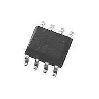
DS90LV028ATM National Semiconductor, DS90LV028ATM Datasheet - Page 4

DS90LV028ATM
Manufacturer Part Number
DS90LV028ATM
Description
IC, LVDS DIFF LINE RECEIVER, SOIC-8
Manufacturer
National Semiconductor
Datasheet
1.DS90LV028ATM.pdf
(10 pages)
Specifications of DS90LV028ATM
Supply Current
5.4mA
Supply Voltage Range
3V To 3.6V
Driver Case Style
SOIC
No. Of Pins
8
Operating Temperature Range
-40°C To +85°C
Device Type
Differential Line Receiver
Current Rating
5.4mA
Data Rate Max
400Mbps
Rohs Compliant
No
Lead Free Status / RoHS Status
Contains lead / RoHS non-compliant
Available stocks
Company
Part Number
Manufacturer
Quantity
Price
Company:
Part Number:
DS90LV028ATM
Manufacturer:
NS
Quantity:
1
Company:
Part Number:
DS90LV028ATM
Manufacturer:
NSC
Quantity:
3 005
Part Number:
DS90LV028ATM
Manufacturer:
NS/国半
Quantity:
20 000
Company:
Part Number:
DS90LV028ATM/NOPB
Manufacturer:
LT
Quantity:
32
Part Number:
DS90LV028ATMX
Manufacturer:
NS/国半
Quantity:
20 000
www.national.com
Applications Information
configurations are possible such as a multi-receiver configu-
ration, but the effects of a mid-stream connector(s), cable
stub(s), and other impedance discontinuities as well as
ground shifting, noise margin limits, and total termination
loading must be taken into account.
The DS90LV028A differential line receiver is capable of de-
tecting signals as low as 100 mV, over a
range centered around +1.2V. This is related to the driver
offset voltage which is typically +1.2V. The driven signal is
centered around this voltage and may shift
center point. The
potential difference between the driver’s ground reference
and the receiver’s ground reference, the common-mode ef-
fects of coupled noise, or a combination of the two. The AC
parameters of both receiver input pins are optimized for a
recommended operating input voltage range of 0V to +2.4V
(measured from each pin to ground). The device will operate
for receiver input voltages up to V
turn on the ESD protection circuitry which will clamp the bus
voltages.
POWER DECOUPLING RECOMMENDATIONS
Bypass capacitors must be used on power pins. Use high
frequency ceramic (surface mount is recommended) 0.1µF
and 0.01µF capacitors in parallel at the power supply pin
with the smallest value capacitor closest to the device supply
pin. Additional scattered capacitors over the printed circuit
board will improve decoupling. Multiple vias should be used
to connect the decoupling capacitors to the power planes. A
10µF (35V) or greater solid tantalum capacitor should be
connected at the power entry point on the printed circuit
board between the supply and ground.
PC BOARD CONSIDERATIONS
Use at least 4 PCB board layers (top to bottom): LVDS
signals, ground, power, TTL signals.
Isolate TTL signals from LVDS signals, otherwise the TTL
signals may couple onto the LVDS lines. It is best to put TTL
and LVDS signals on different layers which are isolated by a
power/ground plane(s).
Keep drivers and receivers as close to the (LVDS port side)
connectors as possible.
For PC board considerations for the LLP package, please
refer to application note AN-1187 “Leadless Leadframe
Package.” It is important to note that to optimize signal
integrity (minimize jitter and noise coupling), the LLP thermal
land pad, which is a metal (normally copper) rectangular
region located under the package as seen in Figure 4,
should be attached to ground and match the dimensions of
the exposed pad on the PCB (1:1 ratio).
±
1V shifting may be the result of a ground
CC
, but exceeding V
±
1V common-mode
±
(Continued)
1V around this
CC
will
4
DIFFERENTIAL TRACES
Use controlled impedance traces which match the differen-
tial impedance of your transmission medium (ie. cable) and
termination resistor. Run the differential pair trace lines as
close together as possible as soon as they leave the IC
(stubs should be
reflections and ensure noise is coupled as common-mode.
In fact, we have seen that differential signals which are 1mm
apart radiate far less noise than traces 3mm apart since
magnetic field cancellation is much better with the closer
traces. In addition, noise induced on the differential lines is
much more likely to appear as common-mode which is re-
jected by the receiver.
Match electrical lengths between traces to reduce skew.
Skew between the signals of a pair means a phase differ-
ence between signals which destroys the magnetic field
cancellation benefits of differential signals and EMI will re-
sult! (Note that the velocity of propagation, v = c/E
(the speed of light) = 0.2997mm/ps or 0.0118 in/ps). Do not
rely solely on the autoroute function for differential traces.
Carefully review dimensions to match differential impedance
and provide isolation for the differential lines. Minimize the
number of vias and other discontinuities on the line.
Avoid 90˚ turns (these cause impedance discontinuities).
Use arcs or 45˚ bevels.
Within a pair of traces, the distance between the two traces
should be minimized to maintain common-mode rejection of
the receivers. On the printed circuit board, this distance
should remain constant to avoid discontinuities in differential
impedance. Minor violations at connection points are allow-
able.
TERMINATION
Use a termination resistor which best matches the differen-
tial impedance or your transmission line. The resistor should
be between 90Ω and 130Ω. Remember that the current
mode outputs need the termination resistor to generate the
differential voltage. LVDS will not work correctly without re-
sistor termination. Typically, connecting a single resistor
across the pair at the receiver end will suffice.
Surface mount 1% - 2% resistors are the best. PCB stubs,
component lead, and the distance from the termination to the
receiver inputs should be minimized. The distance between
the termination resistor and the receiver should be
(12mm MAX).
FIGURE 4. LLP Thermal Land Pad and Pin Pads
<
10mm long). This will help eliminate
10007726
r
<
where c
10mm


