EPM7256BTC100-10 Altera, EPM7256BTC100-10 Datasheet
EPM7256BTC100-10
Specifications of EPM7256BTC100-10
Available stocks


Related parts for EPM7256BTC100-10


EPM7256BTC100-10 Summary of contents
Page 1
... FSU t (ns) 2.4 CO1 f (MHz) 303.0 CNT Altera Corporation DS-MAX7000B-3.5 ® High-performance 2.5-V CMOS EEPROM-based programmable logic devices (PLDs) built on second-generation Multiple Array MatriX ® (MAX ) architecture (see Table – Pin-compatible with the popular 5.0-V MAX 7000S and 3.3-V MAX 7000A device families – ...
Page 2
... FineLine BGA, and plastic J-lead chip carrier (PLCC) packages – Pin-compatibility with other MAX 7000B devices in the same package Advanced software support – Software design support and automatic place-and-route provided by Altera’s MAX+PLUS Windows-based PCs and Sun SPARCstation, and HP 9000 Series 700/800 workstations TM , 0.8-mm Ultra ® II development system for ...
Page 3
... Code File (.jbc), or Serial Vector Format File (.svf)-capable in- circuit tester Table 2. Table 2. MAX 7000B Speed Grades Device - Contact Altera Marketing for up-to-date information on available device speed grades. TM serial/universal serial bus (USB) TM parallel port TM STAPL File (.jam), Jam Byte- Note (1) Speed Grade ...
Page 4
... Contact Altera for up-to-date information on available device package options. (3) All 0.8-mm Ultra FineLine BGA packages are footprint-compatible via the SameFrame designers can design a board to support a variety of devices, providing a flexible migration path across densities and pin counts. Device migration is fully supported by Altera development tools. See page 14 for more details. (4) All FineLine BGA packages are footprint-compatible via the SameFrame pin-out feature ...
Page 5
... MAX 7000B devices to be used in mixed-voltage systems. MAX 7000B devices are supported by Altera development systems, which are integrated packages that offer schematic, text—including VHDL, Verilog HDL, and the Altera Hardware Description Language (AHDL)— ...
Page 6
... PIA that are used for general logic inputs Global controls that are used for secondary register functions Direct input paths from I/O pins to the registers that are used for fast setup times Output Enables (1) LAB Macrocells I Control Block LAB Macrocells I Control Block Altera Corporation I I/O ...
Page 7
... XOR gates) to implement combinatorial functions secondary inputs to the macrocell’s register preset, clock, and clock enable control functions. Two kinds of expander product terms (“expanders”) are available to supplement macrocell logic resources: ■ ■ Altera Corporation MAX 7000B Programmable Logic Device Data Sheet Figure 2 Global Global Clear Clocks ...
Page 8
... MAX 7000B Programmable Logic Device Data Sheet The Altera development system automatically optimizes product-term allocation according to the logic requirements of the design. For registered functions, each macrocell flipflop can be individually programmed to implement operation with programmable clock control. The flipflop can be bypassed for combinatorial operation. ...
Page 9
... A small delay (t shareable expanders are used. can feed multiple macrocells. Figure 3. MAX 7000B Shareable Expanders Shareable expanders can be shared by any or all macrocells in an LAB. Altera Corporation MAX 7000B Programmable Logic Device Data Sheet Figure 3 36 Signals 16 Shared ...
Page 10
... OR logic, with five product terms provided by the macrocell and 15 parallel expanders provided by neighboring macrocells in the LAB. The Altera Compiler can automatically allocate up to three sets five parallel expanders to the macrocells that require additional product terms. Each set of five parallel expanders incurs a small, incremental ...
Page 11
... Only the signals required by each LAB are actually routed from the PIA into the LAB. into the LAB. An EEPROM cell controls one input to a two-input AND gate, which selects a PIA signal to drive into the LAB. Altera Corporation MAX 7000B Programmable Logic Device Data Sheet From Previous ...
Page 12
... MAX 7000B devices. The I/O control block has six or ten global output enable signals that are driven by the true or complement of two output enable signals, a subset of the I/O pins subset of the I/O macrocells. 12 PIA Signals To LAB . Figure 6 shows the I/O CC Altera Corporation ...
Page 13
... The MAX 7000B architecture provides dual I/O feedback, in which macrocell and pin feedbacks are independent. When an I/O pin is configured as an input, the associated macrocell can be used for buried logic. Altera Corporation MAX 7000B Programmable Logic Device Data Sheet Global Output Enable Signals (1) ...
Page 14
... FineLine BGA package. The Altera software provides support to design PCBs with SameFrame pin-out devices. Devices can be defined for present and future use. The Altera software generates pin-outs describing how to layout a board to take advantage of this migration (see Figure 7. SameFrame Pin-Out Example ...
Page 15
... PCB with standard pick-and-place equipment before they are programmed. MAX 7000B devices can be programmed by downloading the information via in-circuit testers, embedded processors, the Altera MasterBlaster communications cable, and the ByteBlasterMV parallel port download cable. Programming the devices after they are placed on the board eliminates lead damage on high-pin-count packages (e ...
Page 16
... EEPROM cells. This process is repeated for each EEPROM address. Verify. Verifying an Altera device in-system involves shifting in addresses, applying the read pulse to verify the EEPROM cells, and shifting out the data for comparison. This process is repeated for each EEPROM address ...
Page 17
... The time required to program a single MAX 7000B device in-system can be calculated from the following formula: t PROG where: t The ISP times for a stand-alone verification of a single MAX 7000B device can be calculated from the following formula: t VER where: t Altera Corporation MAX 7000B Programmable Logic Device Data Sheet Cycle PTCK = t + ------------------------------- - PPULSE f ...
Page 18
... Altera Corporation Cycle VTCK 18,000 35,000 69,000 151,000 300,000 Units 50 kHz 3.52 s 4.52 s 6.56 s 11.44 s 20.40 s Units 50 kHz ...
Page 19
... For more information, see the The Altera software can use text- or waveform-format test vectors created with the Altera Text Editor or Waveform Editor to test the programmed device. For added design verification, designers can perform functional testing to compare the functional device behavior with the results of simulation ...
Page 20
... The most significant bit (MSB the left. The least significant bit (LSB) for all JTAG IDCODEs is 1. Application Note 39 (IEEE 1149.1 (JTAG) Boundary-Scan Testing in Altera for more information on JTAG boundary-scan testing. shows the timing information for the JTAG signals. ...
Page 21
... Figure 8. MAX 7000B JTAG Waveforms Captured Table 9 devices. Symbol Note: (1) Altera Corporation MAX 7000B Programmable Logic Device Data Sheet TMS TDI t JCP t t JCH JCL TCK t JPZX TDO t JSSU Signal JSZX Signal to Be Driven shows the JTAG timing parameters and values for MAX 7000B Table 9. JTAG Timing Parameters & ...
Page 22
... VCCIO pins are connected to a 3.3-V power supply, the output high is at 3.3 V and is therefore compatible with 3.3-V or 5.0-V systems. Devices operating with V adder. Table and t parameters. EN SEXP levels of 2 1.8 V incur a nominal timing delay CCIO describes the MAX 7000B MultiVolt I/O support. ) for the LPA LAD LAC IC ACL Altera Corporation , CC ...
Page 23
... Advanced I/O Standard Support The MAX 7000B I/O pins support the following I/O standards: LVTTL, LVCMOS, 1.8-V I/O, 2.5-V I/O, GTL+, SSTL-3 Class I and II, and SSTL-2 Class I and II. Altera Corporation MAX 7000B Programmable Logic Device Data Sheet Input Signal (V) 2.5 3.3 5 ...
Page 24
... Table 11. Macrocell Pins Contained in Each I/O Bank Device EPM7032B EPM7064B EPM7128B EPM7256B EPM7512B level. Any I/O pin that uses one of the voltage-referenced standards REF Individual Power Bus Bank 1 Bank 2 1-16 17-32 1-32 33-64 1-64 65-128 1-128, 177-181 129-176, 182-256 1-265 266-512 Altera Corporation ...
Page 25
... V recommended operation conditions. When transitioning from ISP to User Mode with bus hold enabled, the bus-hold circuit captures the value present on the pin at the end of programming. Altera Corporation MAX 7000B Programmable Logic Device Data Sheet level. CCIO to prevent overdriving signals ...
Page 26
... Input Setup Time to CLK—Bused Signal parameter. However, these devices are within that parameter. EPM7256B and EPM7512B devices meet all other 66-MHz PCI timing specifications. Drive to VCCIO level R BH I/O Table 13 shows the MAX 7000B Specification 66-MHz PCI - Altera Corporation (1) (1) ...
Page 27
... EEPROM bit and all internal logic elements ensures 100% programming yield. AC test measurements are taken under conditions equivalent to those shown in erased during early stages of the production flow. Altera Corporation MAX 7000B Programmable Logic Device Data Sheet and V power planes can be powered in any ...
Page 28
... Device Output 600 Ω [481 Ω] Device input rise and fall S2 times < Note (1) Min Max –0.5 3.6 –0.5 3.6 –2.0 4.6 –33 50 –65 150 –65 135 –65 135 Altera Corporation To Test System C1 (includes jig capacitance) Unit ° C ° C ° C ...
Page 29
... Output voltage O T Ambient temperature A T Junction temperature J t Input rise time R t Input fall time F Altera Corporation MAX 7000B Programmable Logic Device Data Sheet Conditions (10) (3) For commercial use For industrial use (11) For commercial use For industrial use (11) Min Max Unit 2 ...
Page 30
... V (8) CCIO Min Max Unit 2.0 3.9 V 1.7 3.9 V × 0.65 3 CCIO –0.5 0.8 V –0.5 0.7 V × –0.5 0.35 V CCIO 2 – V CCIO 0.2 2.1 V 2.0 V 1.7 V 1.2 V 0.4 V 0.2 V 0.2 V 0.4 V 0.7 V 0.4 V μ – μ – k¾ Altera Corporation ...
Page 31
... The device is fully initialized within the POR time after V (11) These devices support in-system programming for –40° to 100° C. For in-system programming support between –40° and 0° C, contact Altera Applications. Altera Corporation MAX 7000B Programmable Logic Device Data Sheet ...
Page 32
... MAX 7000B 2.5-V VCCIO V = 2.5 V Typical I CCINT 3.0 V Output CCI O Room Temperature Current (mA 1.8-V VCCIO 150 I OL 120 CCINT V = 1.8 V CCI O Room Temperature Output Voltage (V) O 150 I OL 120 CCINT V = 2.5 V CCI O Room Temperature Output Voltage ( Altera Corporation 3 4 ...
Page 33
... Timing Model MAX 7000B device timing can be analyzed with the Altera software, with a variety of popular industry-standard EDA simulators and timing analyzers, or with the timing model shown in devices have predictable internal delays that enable the designer to determine the worst-case timing of any design. The Altera software provides timing simulation, point-to-point delay prediction, and detailed timing analysis for device-wide performance evaluation ...
Page 34
... GLOB Global Clock at Register Array Clock Mode ACH Clock into PIA t PIA Clock into Logic Array Clock at Register Data from Logic Array t to Logic Array to Pin t PIA t SEXP LAC LAD t PEXP t COMB ACL PIA CLR t OD Altera Corporation PIA PRE t OD ...
Page 35
... CNT period f Maximum internal global CNT clock frequency t Minimum array clock ACNT period f Maximum internal array ACNT clock frequency Altera Corporation MAX 7000B Programmable Logic Device Data Sheet through 32 show MAX 7000B device timing parameters. Notes (1) Conditions -3.5 Min Max (2) 3 (2) 3 ...
Page 36
... Altera Corporation Unit ...
Page 37
... Input to global clock and clear Input to fast input register All outputs GTL+ Input to PIA Input to global clock and clear Input to fast input register All outputs Altera Corporation MAX 7000B Programmable Logic Device Data Sheet Parameter -3.5 Min Notes (1) Speed Grade -5.0 -7 ...
Page 38
... LAD LAC IC ACL CPPW Notes (1) Speed Grade -5.0 -7.5 Max Min Max Min 0.0 0.0 0.0 0.0 0.0 0.0 0.0 0.0 Table 15 on page 29. See , t , and t parameters for macrocells EN SEXP Altera Corporation Unit Max 0.0 ns 0.0 ns 0.0 ns 0.0 ns Figure 14 for ...
Page 39
... Minimum global clock CNT period f Maximum internal global CNT clock frequency t Minimum array clock ACNT period f Maximum internal array ACNT clock frequency Altera Corporation MAX 7000B Programmable Logic Device Data Sheet Note (1) Conditions -3 Min Max (2) 3 (2) 3.5 (2) 2.1 0.0 (2) 1 ...
Page 40
... Altera Corporation Unit ...
Page 41
... Input to PIA Input to global clock and clear Input to fast input register All outputs GTL+ Input to PIA Input to global clock and clear Input to fast input register All outputs Altera Corporation MAX 7000B Programmable Logic Device Data Sheet Parameter -3 Min Note (1) Speed Grade -5 -7 ...
Page 42
... Parameter -3 Min , LAD LAC IC ACL CPPW Note (1) Speed Grade -5 -7 Max Min Max Min 0.0 0.0 0.0 0.0 0.0 0.0 0.0 0.0 Table 15 on page 29. See , t , and t parameters for macrocells EN SEXP Altera Corporation Unit Max 0.0 ns 0.0 ns 0.0 ns 0.0 ns Figure 14 for ...
Page 43
... Minimum global clock CNT period f Maximum internal global CNT clock frequency t Minimum array clock ACNT period f Maximum internal array ACNT clock frequency Altera Corporation MAX 7000B Programmable Logic Device Data Sheet Note (1) Conditions -4 Min Max (2) 4 (2) 4.0 (2) 2.5 0.0 (2) 1 ...
Page 44
... Altera Corporation Unit ...
Page 45
... Input to PIA Input to global clock and clear Input to fast input register All outputs GTL+ Input to PIA Input to global clock and clear Input to fast input register All outputs Altera Corporation MAX 7000B Programmable Logic Device Data Sheet Parameter -4 Min Note (1) Speed Grade -7 -10 ...
Page 46
... Parameter -4 Min , LAD LAC IC ACL CPPW Note (1) Speed Grade -7 -10 Max Min Max Min 0.0 0.0 0.0 0.0 0.0 0.0 0.0 0.0 Table 15 on page 29. See , t , and t parameters for macrocells EN SEXP Altera Corporation Unit Max 0.0 ns 0.0 ns 0.0 ns 0.0 ns Figure 14 for ...
Page 47
... Minimum global clock CNT period f Maximum internal global CNT clock frequency t Minimum array clock ACNT period f Maximum internal array ACNT clock frequency Altera Corporation MAX 7000B Programmable Logic Device Data Sheet Note (1) Conditions -5 Min Max (2) 5 (2) 5.0 (2) 3.3 (2) 0.0 1 ...
Page 48
... Altera Corporation Unit ...
Page 49
... Input to PIA Input to global clock and clear Input to fast input register All outputs GTL+ Input to PIA Input to global clock and clear Input to fast input register All outputs Altera Corporation MAX 7000B Programmable Logic Device Data Sheet Parameter -5 Min Note (1) Speed Grade -7 -10 ...
Page 50
... Parameter -5 Min , LAD LAC IC ACL CPPW Note (1) Speed Grade -7 -10 Max Min Max Min 0.0 0.0 0.0 0.0 0.0 0.0 0.0 0.0 Table 15 on page 29. See , t , and t parameters for macrocells EN SEXP Altera Corporation Unit Max 0.0 ns 0.0 ns 0.0 ns 0.0 ns Figure 14 for ...
Page 51
... Minimum global clock CNT period f Maximum internal global CNT clock frequency t Minimum array clock ACNT period f Maximum internal array ACNT clock frequency Altera Corporation MAX 7000B Programmable Logic Device Data Sheet Note (1) Conditions -5 Min Max (2) 5 (2) 5.5 (2) 3.6 0.0 (2) 1 ...
Page 52
... Altera Corporation Unit ...
Page 53
... Input to PIA Input to global clock and clear Input to fast input register All outputs GTL+ Input to PIA Input to global clock and clear Input to fast input register All outputs Altera Corporation MAX 7000B Programmable Logic Device Data Sheet Parameter -5 Min Note (1) Speed Grade -7 -10 ...
Page 54
... LPA running in low-power mode. Power Supply power (P) versus frequency (f devices is calculated with the following equation: Consumption The P and switching frequency, can be calculated using the guidelines given in Application Note 74 (Evaluating Power for Altera Devices). 54 Parameter -5 Min , LAD LAC ...
Page 55
... LAB with no output load. Actual I because this measurement is sensitive to the actual pattern in the device and the environmental operating conditions. Altera Corporation MAX 7000B Programmable Logic Device Data Sheet value depends on the switching frequency and the application CCINT ...
Page 56
... CC 90 VCC = 2.5 V Room Temperature Typical I CC Active (mA 100 EPM7032B High Speed 153.8 MHz Low Power 250 150 200 Frequency (MHz) EPM7064B High Speed 153.8 MHz Low Power 150 200 250 Frequency (MHz) Altera Corporation 285.7 MHz 300 285.7 MHz 300 ...
Page 57
... Figure 17. I Figure 18. I Altera Corporation MAX 7000B Programmable Logic Device Data Sheet vs. Frequency for EPM7128B Devices CC 220 VCC = 2.5 V 200 Room Temperature 180 160 140 Typical I CC 120 Active (mA) 100 100 vs. Frequency for EPM7256B Devices CC 400 VCC = 2.5 V Room Temperature ...
Page 58
... MAX 7000B Programmable Logic Device Data Sheet Figure 19 vs. Frequency for EPM7512B Devices CC 700 VCC = 2.5 V Room Temperature 600 500 400 Typical I CC Active (mA) 300 Low Power 200 100 EPM7512B 163.9 MHz High Speed 99.0 MHz 80 100 120 140 160 180 Frequency (MHz) Altera Corporation ...
Page 59
... Device See the Altera web site (http://www.altera.com) or the Altera Digital Library for pin-out information. Pin-Outs Figures 20 MAX 7000B devices. Figure 20. 44-Pin PLCC/TQFP Package Pin-Out Diagram Package outlines not drawn to scale I/O /TDI 8 I/O 9 I/O 10 GND 11 I/O EPM7032B 12 I/O 13 I/O/TMS EPM7064B ...
Page 60
... Package outlines not drawn to scale N/C I/O/TDI 2 I/O 3 I/O 4 GNDIO 5 I/O / VREFA 6 7 I/O 8 I/O/TMS I/O 9 VCCIO1 48-Pin VTQFP EPM7032B EPM7064B G EPM7128B 36 I/O 35 I/O/TDO 34 I/O 33 I/O 32 VCCIO2 31 I/O EPM7032B 30 I/O EPM7064B 29 I/O/TCK 28 I/O / VREFB 27 GNDIO 26 I/O 25 I/O A1 Ball Pad Corner Altera Corporation ...
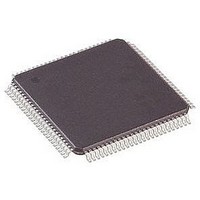
Page 61
... Figure 23. 100-Pin TQFP Package Pin-Out Diagram Figure 24. 100-Pin FineLine BGA Package Pin-Out Diagram Package outline not drawn to scale. Indicates location of Ball A1 Altera Corporation MAX 7000B Programmable Logic Device Data Sheet Package outline not drawn to scale. Pin 1 Pin 26 EPM7064B EPM7128B EPM7256B Pin 76 ...
Page 62
... Figure 25. 144-Pin TQFP Package Pin-Out Diagram Figure 26. 169-Pin Ultra FineLine BGA Pin-Out Diagram Package outline not drawn to scale. Indicates Location of Ball A1 EPM7128AE 62 . Package outline not drawn to scale Indicates location of Pin 1 Pin 1 Pin Pin 109 EPM7128B EPM7256B EPM7512B Pin Altera Corporation A1 Ball Pad Corner ...
Page 63
... Figure 27. 208-Pin PQFP Package Pin-Out Diagram Package outline not drawn to scale Pin 1 Pin 53 Altera Corporation MAX 7000B Programmable Logic Device Data Sheet . EPM7256B EPM7512B Pin 157 Pin 105 63 ...
Page 64
... MAX 7000B Programmable Logic Device Data Sheet Figure 28. 256-Pin BGA Package Pin-Out Diagram Package outline not drawn to scale. Indicates Location of Ball A1 EPM7512B Altera Corporation A1 Ball Pad Corner ...
Page 65
... The following changes were made to the MAX 7000B Programmable Logic Device Family Data Sheet version 3.5: ■ Version 3.4 The following changes were made to the MAX 7000B Programmable Logic Device Family Data Sheet version 3.4: ■ Altera Corporation MAX 7000B Programmable Logic Device Data Sheet . ...
Page 66
... Copyright © 2003 Altera Corporation. All rights reserved. Altera, The Programmable Solutions Company, the (408) 544-7000 stylized Altera logo, specific device designations, and all other words and logos that are identified as http://www.altera.com trademarks and/or service marks are, unless noted otherwise, the trademarks and service marks of Altera Applications Hotline: Corporation in the U ...