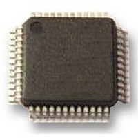
UPD78F0413GA-GAM-AX NEC, UPD78F0413GA-GAM-AX Datasheet - Page 328

UPD78F0413GA-GAM-AX
Manufacturer Part Number
UPD78F0413GA-GAM-AX
Description
8BIT UC, 32K FLASH, 1KB RAM, LCD
Manufacturer
NEC
Datasheet
1.UPD78F0413GA-GAM-AX.pdf
(562 pages)
Specifications of UPD78F0413GA-GAM-AX
Controller Family/series
UPD78F
No. Of I/o's
30
Ram Memory Size
1024Byte
Cpu Speed
10MHz
No. Of Timers
8
No. Of Pwm
RoHS Compliant
Core Size
8bit
Program Memory Size
32KB
Oscillator Type
External, Internal
Available stocks
Company
Part Number
Manufacturer
Quantity
Price
Company:
Part Number:
UPD78F0413GA-GAM-AX
Manufacturer:
ADI
Quantity:
882
Company:
Part Number:
UPD78F0413GA-GAM-AX
Manufacturer:
Renesas Electronics America
Quantity:
10 000
- Current page: 328 of 562
- Download datasheet (4Mb)
328
(d) Reception
R
X
D0 (input)
Reception is enabled and the R
interface operation mode register 0 (ASIM0) is set to 1 and then bit 5 (RXE0) of ASIM0 is set to 1.
The 5-bit counter of the baud rate generator starts counting when the falling edge of the R
detected. When the set value of baud rate generator control register 0 (BRGC0) has been counted, the
R
as a start bit.
When the start bit is detected, reception is started, and serial data is sequentially stored in receive shift
register 0 (RXS0) at the set baud rate. When the stop bit has been received, the reception completion
interrupt (INTSR0) is generated and the data of RXS0 is written to receive buffer register 0 (RXB0). If an
overrun error (OVE0) occurs, however, the receive data is not written to RXB0.
Even if a parity error (PE0) occurs while reception is in progress, reception continues to the reception
position of the stop bit, and an reception error interrupt (INTSR0) is generated after completion of reception.
INTSR0 occurs upon completion of reception and in case of a reception error.
Cautions 1. If a reception error occurs, read asynchronous serial interface reception error status
INTSR0
X
RXB0
D0 pin input is sampled again (
2. Reception is always performed with the “number of stop bits = 1”. The second stop bit
register 0 (ASIS0) and then read receive buffer register 0 (RXB0) to clear the error flag.
Otherwise, an overrun error will occur when the next data is received, and the reception
error status will persist.
is ignored.
Figure 13-10. Reception Completion Interrupt Request Timing
Start
D0
CHAPTER 13 SERIAL INTERFACE UART0
D1
X
D0 pin input is sampled when bit 7 (POWER0) of asynchronous serial
in Figure 13-10). If the R
User’s Manual U18698EJ1V0UD
D2
D3
D4
D5
X
D0 pin is low level at this time, it is recognized
D6
D7
Parity
Stop
X
D0 pin input is
Related parts for UPD78F0413GA-GAM-AX
Image
Part Number
Description
Manufacturer
Datasheet
Request
R

Part Number:
Description:
16/8 bit single-chip microcomputer
Manufacturer:
NEC
Datasheet:

Part Number:
Description:
Dual audio power amp circuit
Manufacturer:
NEC
Datasheet:

Part Number:
Description:
Dual comparator
Manufacturer:
NEC
Datasheet:

Part Number:
Description:
MOS type composite field effect transistor
Manufacturer:
NEC
Datasheet:

Part Number:
Description:
50 V/100 mA FET array incorporating 2 N-ch MOSFETs
Manufacturer:
NEC
Datasheet:

Part Number:
Description:
6-pin small MM high-frequency double transistor
Manufacturer:
NEC
Datasheet:

Part Number:
Description:
6-pin small MM high-frequency double transistor
Manufacturer:
NEC
Datasheet:

Part Number:
Description:
6-pin small MM high-frequency double transistor
Manufacturer:
NEC
Datasheet:

Part Number:
Description:
6-pin small MM high-frequency double transistor
Manufacturer:
NEC
Datasheet:

Part Number:
Description:
Twin transistors equipped with different model chips(6P small MM)
Manufacturer:
NEC
Datasheet:

Part Number:
Description:
Bipolar analog integrated circuit
Manufacturer:
NEC
Datasheet:


