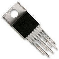
LM2679T-5.0 National Semiconductor, LM2679T-5.0 Datasheet - Page 13

LM2679T-5.0
Manufacturer Part Number
LM2679T-5.0
Description
IC, STEP-DOWN REGULATOR, TO-220-7
Manufacturer
National Semiconductor
Datasheet
1.LM2679S-3.3.pdf
(26 pages)
Specifications of LM2679T-5.0
Primary Input Voltage
12V
No. Of Outputs
1
Output Voltage
5V
Output Current
5A
No. Of Pins
7
Operating Temperature Range
-40°C To +125°C
Supply Voltage Range
8V To 40V
Lead Free Status / RoHS Status
Contains lead / RoHS non-compliant
Available stocks
Company
Part Number
Manufacturer
Quantity
Price
Part Number:
LM2679T-5.0/NOPB
Manufacturer:
NS/国半
Quantity:
20 000
Step 8: Define a value for R
limit to be at least 20% greater than Iout max to allow for at
least 30% inductor ripple current (±15% of Iout). For designs
that must operate over the full temperature range the switch
current limit should be set to at least 50% greater than Iout
max (1.5 x I
FIXED OUTPUT VOLTAGE DESIGN EXAMPLE
A system logic power supply bus of 3.3V is to be generated
from a wall adapter which provides an unregulated DC volt-
age of 13V to 16V. The maximum load current is 4A. A
softstart delay time of 50mS is desired. Through-hole com-
ponents are preferred.
Step 1: Operating conditions are:
Vout = 3.3V
Vin max = 16V
Iload max = 4A
Step 2: Select an LM2679T-3.3. The output voltage will have
a tolerance of
±2% at room temperature and ±3% over the full operating
temperature range.
Step 3: Use the nomograph for the 3.3V device ,Figure 3. The
intersection of the 16V horizontal line (V
vertical line (I
required.
From Table 1, L46 in a through-hole component is available
from Renco with part number RL-1283-15-43.
Step 4: Use Table 3 to determine an output capacitor. With a
3.3V output and a 15μH inductor there are four through-hole
output capacitor solutions with the number of same type ca-
pacitors to be paralleled and an identifying capacitor code
given. Table 2 provides the actual capacitor characteristics.
Any of the following choices will work in the circuit:
2 x 220μF/10V Sanyo OS-CON (code C5)
2 x 820μF/16V Sanyo MV-GX (code C5)
1 x 3900μF/10V Nichicon PL (code C7)
2 x 560μF/35V Panasonic HFQ (code C5)
Step 5: Use Table 4 to select an input capacitor. With 3.3V
output and 15μH there are three through-hole solutions.
These capacitors provide a sufficient voltage rating and an
rms current rating greater than 2A (1/2 I
Table 2 for specific component characteristics the following
choices are suitable:
2 x 680μF/63V Sanyo MV-GX (code C13)
1 x 1200μF/63V Nichicon PL (code C25)
1 x 1500μF/63V Panasonic HFQ (code C16)
Step 6: From Table 5 a 5A or more Schottky diode must be
selected. For through-hole components only 40V rated
diodes are indicated and 4 part types are suitable:
1N5825
MBR745
80SQ045
6TQ045
Step 7: A 0.01μF capacitor will be used for Cboost. For the
50mS softstart delay the following parameters are to be used:
I
t
V
V
V
V
SST
SS
SST
OUT
SCHOTTKY
IN
: 50mS
: 16V
: 3.7μA
: 0.63V
: 3.3V
: 0.5V
out
load
max).
max) indicates that L46, a 15μH inductor, is
ADJ
to set the peak switch current
load
in
max). Again using
max) and the 4A
13
Using Vin max ensures that the softstart delay time will be at
least the desired 50mS.
Using the formula for Css a value of 0.148μF is determined
to be required. Use of a standard value 0.22μF capacitor will
produce more than sufficient softstart delay.
Step 8: Determine a value for R
current limit of at least 4A plus 50% or 6A.
Use a value of 6.2KΩ.
ADJUSTABLE OUTPUT DESIGN EXAMPLE
In this example it is desired to convert the voltage from a two
battery automotive power supply (voltage range of 20V to
28V, typical in large truck applications) to the 14.8VDC alter-
nator supply typically used to power electronic equipment
from single battery 12V vehicle systems. The load current re-
quired is 3.5A maximum. It is also desired to implement the
power supply with all surface mount components. Softstart is
not required.
Step 1: Operating conditions are:
Vout = 14.8V
Vin max = 28V
Iload max = 3.5A
Step 2: Select an LM2679S-ADJ. To set the output voltage
to 14.9V two resistors need to be chosen (R1 and R2 in Figure
2). For the adjustable device the output voltage is set by the
following relationship:
Where V
A recommended value to use for R1 is 1K. In this example
then R2 is determined to be:
R2 = 11.23KΩ
The closest standard 1% tolerance value to use is 11.3KΩ
This will set the nominal output voltage to 14.88V which is
within 0.5% of the target value.
Step 3: To use the nomograph for the adjustable device, Fig-
ure 6, requires a calculation of the inductor Volt•microsecond
constant (E•T expressed in V•μS) from the following formula:
where V
switch which is R
be typically 0.12Ω x 3.5A or 0.42V and V
across the forward bisased Schottky diode, typically 0.5V.
The switching frequency of 260KHz is the nominal value to
use to estimate the ON time of the switch during which energy
is stored in the inductor.
For this example E•T is found to be:
SAT
FB
is the feedback voltage of typically 1.21V.
is the voltage drop across the internal power
ds(ON)
times I
load
ADJ
. In this example this would
to provide a peak switch
D
is the voltage drop
www.national.com


