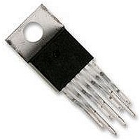
LM2679T-5.0 National Semiconductor, LM2679T-5.0 Datasheet - Page 9

LM2679T-5.0
Manufacturer Part Number
LM2679T-5.0
Description
IC, STEP-DOWN REGULATOR, TO-220-7
Manufacturer
National Semiconductor
Datasheet
1.LM2679S-3.3.pdf
(26 pages)
Specifications of LM2679T-5.0
Primary Input Voltage
12V
No. Of Outputs
1
Output Voltage
5V
Output Current
5A
No. Of Pins
7
Operating Temperature Range
-40°C To +125°C
Supply Voltage Range
8V To 40V
Lead Free Status / RoHS Status
Contains lead / RoHS non-compliant
Available stocks
Company
Part Number
Manufacturer
Quantity
Price
Part Number:
LM2679T-5.0/NOPB
Manufacturer:
NS/国半
Quantity:
20 000
Application Hints
The LM2679 provides all of the active functions required for
a step-down (buck) switching regulator. The internal power
switch is a DMOS power MOSFET to provide power supply
designs with high current capability, up to 5A, and highly ef-
ficient operation.
The LM2679 is part of the SIMPLE SWITCHER family of
power converters. A complete design uses a minimum num-
ber of external components, which have been pre-determined
from a variety of manufacturers. Using either this data sheet
or a design software program called LM267X Made Simple
(version 2.0) a complete switching power supply can be de-
signed quickly. The software is provided free of charge and
can be downloaded from National Semiconductor's Internet
site located at http://www.national.com.
SWITCH OUTPUT
This is the output of a power MOSFET switch connected di-
rectly to the input voltage. The switch provides energy to an
inductor, an output capacitor and the load circuitry under con-
trol of an internal pulse-width-modulator (PWM). The PWM
controller is internally clocked by a fixed 260KHz oscillator. In
a standard step-down application the duty cycle (Time ON/
Time OFF) of the power switch is proportional to the ratio of
the power supply output voltage to the input voltage. The volt-
age on pin 1 switches between Vin (switch ON) and below
ground by the voltage drop of the external Schottky diode
(switch OFF).
INPUT
The input voltage for the power supply is connected to pin 2.
In addition to providing energy to the load the input voltage
also provides bias for the internal circuitry of the LM2679. For
guaranteed performance the input voltage must be in the
range of 8V to 40V. For best performance of the power supply
the input pin should always be bypassed with an input ca-
pacitor located close to pin 2.
C BOOST
A capacitor must be connected from pin 3 to the switch output,
pin 1. This capacitor boosts the gate drive to the internal
MOSFET above Vin to fully turn it ON. This minimizes con-
duction losses in the power switch to maintain high efficiency.
The recommended value for C Boost is 0.01μF.
GROUND
This is the ground reference connection for all components in
the power supply. In fast-switching, high-current applications
9
such as those implemented with the LM2679, it is recom-
mended that a broad ground plane be used to minimize signal
coupling throughout the circuit
CURRENT ADJUST
A key feature of the LM2679 is the ability to tailor the peak
switch current limit to a level required by a particular applica-
tion. This alleviates the need to use external components that
must be physically sized to accommodate current levels (un-
der shorted output conditions for example) that may be much
higher than the normal circuit operating current requirements.
A resistor connected from pin 5 to ground establishes a cur-
rent (I
the power switch. The maximum switch current is fixed at a
level of 37,125 / R
FEEDBACK
This is the input to a two-stage high gain amplifier, which
drives the PWM controller. It is necessary to connect pin 6 to
the actual output of the power supply to set the dc output volt-
age. For the fixed output devices (3.3V, 5V and 12V outputs),
a direct wire connection to the output is all that is required as
internal gain setting resistors are provided inside the LM2679.
For the adjustable output version two external resistors are
required to set the dc output voltage. For stable operation of
the power supply it is important to prevent coupling of any
inductor flux to the feedback input.
SOFTSTART
A capacitor connected from pin 7 to ground allows for a slow
turn-on of the switching regulator. The capacitor sets a time
delay to gradually increase the duty cycle of the internal power
switch. This can significantly reduce the amount of surge cur-
rent required from the input supply during an abrupt applica-
tion of the input voltage. If softstart is not required this pin
should be left open circuited. Please see the C
pacitor section for further information regarding softstart ca-
pacitor values.
DAP (LLP PACKAGE)
The Die Attach Pad (DAP) can and should be connected to
PCB Ground plane/island. For CAD and assembly guidelines
refer
power.national.com.
(pin 5)
to
= 1.2V / R
Application
ADJ
.
ADJ
) that sets the peak current through
Note
AN-1187
SS
www.national.com
softstart ca-
at
http://


