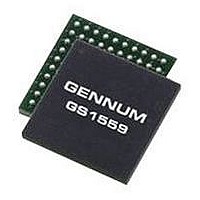
GS1559CBE2 GENNUM, GS1559CBE2 Datasheet - Page 27

GS1559CBE2
Manufacturer Part Number
GS1559CBE2
Description
IC, DES, 48.5MHZ 20BIT 1.485GBPS BGA-100
Manufacturer
GENNUM
Datasheet
1.GS1559CBE2.pdf
(73 pages)
Specifications of GS1559CBE2
Supply Voltage Range
1.71V To 1.89V, 3.13V To 3.47V
Operating Temperature Range
0°C To +70°C
Digital Ic Case Style
BGA
No. Of Pins
100
Termination Type
SMD
Control Interface
Serial
Lead Free Status / RoHS Status
Lead free / RoHS Compliant
4.2.1 Input Signal Selection
4.2.2 Carrier Detect Input
4.2.3 Single Input Configuration
4.3 Serial Digital Reclocker
A 2x1 input multiplexer is provided to allow the application layer to select between
the two serial digital input streams using a single external pin. When IP_SEL is set
HIGH, serial digital input 1 (DDI1 / DDI1) is selected as the input to the GS1559's
reclocker stage. When IP_SEL is set LOW, serial digital input 2 (DDI2 / DDI2) is
selected.
For each of the differential inputs, an associated carrier detect input signal is
included, (CD1 and CD2). These signals are generated by Gennum's family of
automatic cable equalizers.
When LOW, CDx indicates that a valid serial digital data stream is being delivered
to the GS1559 by the equalizer. When HIGH, the serial digital input to the device
should be considered invalid. If no equalizer precedes the device, the application
layer should set CD1 and CD2 accordingly.
A 2x1 input multiplexer is also provided for these signals. The internal
carrier_detect signal is determined by the setting of the IP_SEL pin and is used by
the lock detect block of the GS1559 to determine the lock status of the device, (see
Lock Detect on page
If the application requires a single differential input, the DDI pin for the second set
of inputs and the associated carrier detect should be tied HIGH. The DDI pin may
be left unconnected, and the termination pin should be AC terminated to ground.
The output of the 2x1 serial digital input multiplexer passes to the GS1559's
internal reclocker stage. The function of this block is to lock to the input data
stream, extract a clean clock, and retime the serial digital data to remove high
frequency jitter.
The reclocker was designed with a 'hexabang' phase and frequency detector. That
is, the PFD used can identify six 'degrees' of phase / frequency misalignment
between the input data stream and the clock signal provided by the VCO, and
correspondingly signal the charge pump to produce six different control voltages.
This results in fast and accurate locking of the PLL to the data stream.
In master mode, the operating center frequency of the reclocker is toggled between
270Mb/s and 1.485Gb/s by the lock detect block, (see
slave mode, however, the center frequency is determined entirely by the SD/HD
input control signal set by the application layer.
If lock is achieved, the reclocker provides an internal pll_lock signal to the lock
detect block of the device.
30572 - 7
May 2007
31).
Lock Detect on page
GS1559 Data Sheet
27 of 73
31). In


