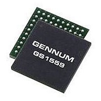
GS1559CBE2 GENNUM, GS1559CBE2 Datasheet - Page 6

GS1559CBE2
Manufacturer Part Number
GS1559CBE2
Description
IC, DES, 48.5MHZ 20BIT 1.485GBPS BGA-100
Manufacturer
GENNUM
Datasheet
1.GS1559CBE2.pdf
(73 pages)
Specifications of GS1559CBE2
Supply Voltage Range
1.71V To 1.89V, 3.13V To 3.47V
Operating Temperature Range
0°C To +70°C
Digital Ic Case Style
BGA
No. Of Pins
100
Termination Type
SMD
Control Interface
Serial
Lead Free Status / RoHS Status
Lead free / RoHS Compliant
- Current page: 6 of 73
- Download datasheet (2Mb)
1.2 Pin Descriptions
Table 1-1: Pin Descriptions
F2, F3, F7,
A8, E8, K8
Number
J2, J3, J4,
G2, G3,
G7, H3,
A6, B5,
B6, C4,
C5, D2,
D3, D7,
E3, E7,
A4, A5
Pin
A1
A2
A3
A7
VCO_GND
VCO_VCC
VCO, VCO
IO_VDD
Name
PCLK
NC
LF
30572 - 7
Timing
Analog
Analog
–
–
–
–
–
May 2007
Output
Output
Output
Output
Power
Power
Power
Type
Input
–
Description
Control voltage to external voltage controlled oscillator. Nominally +1.25V
DC.
Power supply for the external voltage controlled oscillator. Connect to pin 7
of the GO1555/GO1525*. This pin is an output.
Should be isolated from all other power supplies.
*For new designs use GO1555
Ground reference for the external voltage controlled oscillator. Connect to
pins 2, 4, 6, and 8 of the GO1555/GO1525*. This pin is an output.
Should be isolated from all other grounds.
*For new designs use GO1555
Differential inputs for the external VCO reference signal. For single ended
devices such as the GO1555/GO1525*, VCO should be AC coupled to
VCO_GND.
VCO is nominally 1.485GHz.
*For new designs use GO1555
No Connect.
PARALLEL DATA BUS CLOCK
Signal levels are LVCMOS/LVTTL compatible.
HD 20-bit mode
HD 10-bit mode
SD 20-bit mode
SD 10-bit mode
Power supply connection for digital I/O buffers. Connect to +3.3V DC
digital.
PCLK = 74.25MHz or 74.25/1.001MHz
PCLK = 148.5MHz or 148.5/1.001MHz
PCLK = 13.5MHz
PCLK = 27MHz
GS1559 Data Sheet
6 of 73
Related parts for GS1559CBE2
Image
Part Number
Description
Manufacturer
Datasheet
Request
R

Part Number:
Description:
GS1559 HD-LINX-TM II Multi-Rate Deserializer with Loop-Through Cable Driver
Manufacturer:
Gennum Corp.
Datasheet:

Part Number:
Description:
HD-LINX II Multi-Rate Deserializer with Loop-Through Cable Driver
Manufacturer:
Gennum Corp.
Datasheet:

Part Number:
Description:
Wideband, monolithic 1x1 video crosspoint switch
Manufacturer:
Gennum Corporation
Datasheet:

Part Number:
Description:
Wideband, Monolithic 4x1 Video Multiplexer
Manufacturer:
Gennum Corporation
Datasheet:

Part Number:
Description:
Monolithic 4x1 Video Multiplexer
Manufacturer:
Gennum Corporation
Datasheet:

Part Number:
Description:
Low Distortion AGC Amplifier
Manufacturer:
Gennum Corporation
Datasheet:


