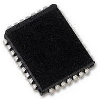
CAT28F010GI-12 CATALYST SEMICONDUCTOR, CAT28F010GI-12 Datasheet - Page 5

CAT28F010GI-12
Manufacturer Part Number
CAT28F010GI-12
Description
IC, FLASH, 1MBIT, 120NS, LCC-32
Manufacturer
CATALYST SEMICONDUCTOR
Datasheet
1.CAT28F010G-12T.pdf
(16 pages)
Specifications of CAT28F010GI-12
Memory Type
Flash
Memory Size
1Mbit
Memory Configuration
128K X 8
Access Time
120ns
Supply Voltage Range
4.5V To 5.5V
Memory Case Style
PLCC
No. Of Pins
32
Lead Free Status / RoHS Status
Lead free / RoHS Compliant
Available stocks
Company
Part Number
Manufacturer
Quantity
Price
Company:
Part Number:
CAT28F010GI-12
Manufacturer:
NEC
Quantity:
6 000
Company:
Part Number:
CAT28F010GI-12T
Manufacturer:
CSI
Quantity:
6 250
Company:
Part Number:
CAT28F010GI-12T
Manufacturer:
ON Semiconductor
Quantity:
10 000
SUPPLY CHARACTERISTICS
A.C. CHARACTERISTICS, Read Operation
V
Note:
(1) This parameter is tested initially and after a design or process change that affects the parameter.
(2) Output floating (High-Z) is defined as the state where the external data line is no longer driven by the output buffer.
(3) Input Rise and Fall Times (10% to 90%) < 10 ns.
(4) Input Pulse Levels = 0.45V and 2.4V. For High Speed Input Pulse Levels 0.0V and 3.0V.
(5) Input and Output Timing Reference = 0.8V and 2.0V. For High Speed Input and Output Timing Reference = 1.5V.
(6) Low-Z is defined as the state where the external data may be driven by the output buffer but may not be valid.
(7)
© 2009 SCILLC. All rights reserved.
Characteristics subject to change without notice
JEDEC Standard
Symbol Symbol
t
WHGL
CC
t
t
t
t
t
t
t
t
t
AVQV
GLQV
AXQX
GLQX
GHQZ
EHQZ
AVAV
ELQV
ELZX
For load and reference points, see Fig. 1
Symbol
= +5V 10%, unless otherwise specified.
V
V
V
(1)
CC
PPL
PPH
t
t
t
OLZ
t
DF
DF
LZ
t
t
t
ACC
t
t
RC
OE
OH
CE
(1)(6)
(1)(2)
(1)(2)
(1)(6)
-
Parameter
Read Cycle Time
CE Access Time
Address Access Time
OE Access Time
Output Hold from Address OE/CE Change
OE to Output in Low-Z
CE to Output in Low-Z
OE High to Output High-Z
CE High to Output High-Z
Write Recovery Time Before Read
V
V
V
CC
PP
PP
During Read Operations
During Read/Erase/Program
Supply Voltage
Figure 1. A.C. Testing Input/Output Waveform
0.45 V
2.4 V
DEVICE
UNDER
TEST
Parameter
Testing Load Circuit (example)
INPUT PULSE LEVELS
5108 FHD F04
1.3V
1N914
3.3K
C L = 100 pF
5
2.0 V
0.8 V
C L INCLUDES JIG CAPACITANCE
OUT
REFERENCE POINTS
Min
90
28F010-90
0
0
0
6
11.4
Min
4.5
0
Max
90
90
35
20
30
(7)
5108 FHD F03
Limits
(3)(4)(5)
28F010-12
Min
120
0
0
0
6
Max.
12.6
5.5
6.5
120
120
Max
50
30
40
(7)
Doc. No. MD-1019, Rev. G
CAT28F010
Unit
Unit
ns
ns
ns
ns
ns
ns
ns
ns
ns
V
V
V
s


