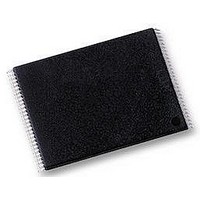
HY27UF084G2B-TPCB HYNIX SEMICONDUCTOR, HY27UF084G2B-TPCB Datasheet - Page 22

HY27UF084G2B-TPCB
Manufacturer Part Number
HY27UF084G2B-TPCB
Description
IC, MEMORY, FLASH NAND 4GB, TSOP48
Manufacturer
HYNIX SEMICONDUCTOR
Datasheet
1.HY27UF084G2B-TPCB.pdf
(51 pages)
Specifications of HY27UF084G2B-TPCB
Access Time
20ns
Supply Voltage Range
2.7V To 3.6V
Memory Case Style
TSOP
No. Of Pins
48
Operating Temperature Range
0°C To +70°C
Package / Case
TSOP
Base Number
27
Interface
Parallel
Logic
RoHS Compliant
Memory Type
Flash - NAND
Memory Configuration
512M X 8
Rohs Compliant
Yes
Available stocks
Company
Part Number
Manufacturer
Quantity
Price
Company:
Part Number:
HY27UF084G2B-TPCB
Manufacturer:
HYNIX
Quantity:
11 250
Company:
Part Number:
HY27UF084G2B-TPCB
Manufacturer:
HYNIX
Quantity:
12 500
Part Number:
HY27UF084G2B-TPCB
Manufacturer:
HYNIX/海力士
Quantity:
20 000
Rev 0.4 / Jan. 2008
DEVICE IDENTIFIER CYCLE
HY27UF084G2B
HY27UF164G2B
Part Number
IO
0
1
2
3
4
5
6
7
Page Program
2nd
3rd
4th
5th
1st
Ready / Busy
Ready / Busy
Write Protect
Pass / Fail
NA
NA
NA
NA
Voltage
3.3V
3.3V
Width
Block Erase
Ready / Busy
Ready / Busy
Write Protect
Bus
x16
x8
Table 14 : Status Register Coding
Pass / Fail
Table 15: Device Identifier Coding
NA
NA
NA
NA
Table 16: Read ID Data Table
(Manufacture Code)
1st cycle
Page Size, Block Size, Spare Size, Organization
ADh
ADh
Ready /
Ready /
Protect
Internal chip number, cell Type, etc.
Read
Write
Busy
Busy
NA
NA
NA
NA
NA
Multiplane information
Manufacturer Code
DESCRIPTION
Device Identifier
4Gbit (512Mx8bit) NAND Flash
(Device Code)
Cache Read
Controller Bit
2nd cycle
Ready/Busy
HY27UF(08/16)4G2B Series
DCh
CCh
P/E/R
NA
NA
NA
NA
NA
NA
cycle
3rd
10h
10h
Busy: ‘0’ Ready:’1’
Not Protected: ‘1’
Active: ‘0’ Idle:’1’
Pass: ‘0’ Fail: ‘1’
Protected: ‘0’
CODING
cycle
4th
D5h
95h
-
-
-
-
cycle
5th
54h
54h
22


