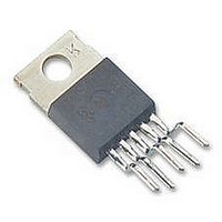
LM2591HVT-3.3 National Semiconductor, LM2591HVT-3.3 Datasheet - Page 14

LM2591HVT-3.3
Manufacturer Part Number
LM2591HVT-3.3
Description
Voltage Regulator IC
Manufacturer
National Semiconductor
Specifications of LM2591HVT-3.3
Output Voltage
3.3VDC
Output Current
1A
No. Of Pins
5
Termination Type
Through Hole
Mounting Type
Through Hole
Peak Reflow Compatible (260 C)
No
Supply Voltage Max
60V
Leaded Process Compatible
No
Lead Free Status / RoHS Status
Contains lead / RoHS non-compliant
www.national.com
Application Information
Therefore, looking at Figure 2 we quick-select a 100µH/1A
inductor (designed for 150 kHz operation) for this applica-
tion.
2. We should confirm that it is rated to handle 100 µJ (see
Figure 4) by the procedure shown in AN-1197 and that the
losses are acceptable. (If the DC Input voltage had been
greater than 40V we would need to consider e
Example 2 above).
Note that we have taken V
estimated resistive drop across the inductor.
This completes the simplified inductor selection procedure.
For more general applications and better optimization, the
designer should refer to AN-1197. Figure 6 provides helpful
contact information on suggested Inductor manufacturers
who may be able to recommend suitable parts, if the require-
ments are known.
FEEDFORWARD CAPACITOR
(Adjustable Output Voltage Version)
C
Figure 1 is used when the output voltage is greater than 10V
or when C
compensation to the feedback loop and increases the phase
margin for better loop stability.
If the output voltage ripple is large (
output voltage), this ripple can be coupled to the feedback
pin through the feedforward capacitor and cause the error
comparator to trigger the error flag. In this situation, adding a
resistor, R
proximately 3 times R1, will attenuate the ripple voltage at
the feedback pin.
INPUT CAPACITOR
C
needed between the input pin and ground pin. It must be
located near the regulator using short leads. This capacitor
prevents large voltage transients from appearing at the in-
put, and provides the instantaneous current needed each
time the switch turns on.
The important parameters for the Input capacitor are the
voltage rating and the RMS current rating. Because of the
relatively high RMS currents flowing in a buck regulator’s
input capacitor, this capacitor should be chosen for its RMS
current rating rather than its capacitance or voltage ratings,
although the capacitance value and voltage rating are di-
rectly related to the RMS current rating. The voltage rating of
the capacitor and its RMS ripple current capability must
never be exceeded.
FF
IN
— A low ESR aluminum or tantalum bypass capacitor is
- A Feedforward Capacitor C
OUT
FF
, in series with the feedforward capacitor, ap-
has a very low ESR. This capacitor adds lead
SAT
as 1.5V which includes an
FF
, shown across R2 in
>
5% of the nominal
(Continued)
CLIM
as in
14
OUTPUT CAPACITOR
C
and provide regulator loop stability. Low impedance or low
ESR Electrolytic or solid tantalum capacitors designed for
switching regulator applications must be used. When select-
ing an output capacitor, the important capacitor parameters
are; the 100 kHz Equivalent Series Resistance (ESR), the
RMS ripple current rating, voltage rating, and capacitance
value. For the output capacitor, the ESR value is the most
important parameter. The ESR should generally not be less
than 100 mΩ or there will be loop instability. If the ESR is too
large, efficiency and output voltage ripple are effected. So
ESR must be chosen carefully.
CATCH DIODE
Buck regulators require a diode to provide a return path for
the inductor current when the switch turns off. This must be
a fast diode and must be located close to the LM2591HV
using short leads and short printed circuit traces.
Because of their very fast switching speed and low forward
voltage drop, Schottky diodes provide the best performance,
especially in low output voltage applications (5V and lower).
Ultra-fast recovery, or High-Efficiency rectifiers are also a
good choice, but some types with an abrupt turnoff charac-
teristic may cause instability or EMI problems. Ultra-fast
recovery diodes typically have reverse recovery times of 50
ns or less. The diode must be chosen for its average/RMS
current rating and maximum voltage rating. The voltage
rating of the diode must be greater than the DC input voltage
(not the output voltage).
DELAYED STARTUP
The circuit in Figure 7 uses the the ON /OFF pin to provide
a time delay between the time the input voltage is applied
and the time the output voltage comes up (only the circuitry
pertaining to the delayed start up is shown). As the input
voltage rises, the charging of capacitor C1 pulls the ON /OFF
pin high, keeping the regulator off. Once the input voltage
reaches its final value and the capacitor stops charging, and
resistor R
circuit to start switching. Resistor R
maximum voltage applied to the ON /OFF pin (maximum of
25V), reduces power supply noise sensitivity, and also limits
the capacitor, C1, discharge current. When high input ripple
voltage exists, avoid long delay time, because this ripple can
be coupled into the ON /OFF pin and cause problems.
This delayed startup feature is useful in situations where the
input power source is limited in the amount of current it can
deliver. It allows the input voltage to rise to a higher voltage
before the regulator starts operating. Buck regulators require
less input current at higher input voltages.
OUT
— An output capacitor is required to filter the output
2
pulls the ON /OFF pin low, thus allowing the
1
is included to limit the


