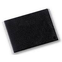
S29AL008D70TFI020 Spansion Inc., S29AL008D70TFI020 Datasheet - Page 11

S29AL008D70TFI020
Manufacturer Part Number
S29AL008D70TFI020
Description
Flash Memory IC
Manufacturer
Spansion Inc.
Datasheet
1.S29AL008D70TFI020.pdf
(55 pages)
Specifications of S29AL008D70TFI020
Memory Size
8Mbit
Memory Configuration
1M X 8 / 512K X 16
Ic Interface Type
Parallel
Access Time
70ns
Memory Case Style
TSOP
No. Of Pins
48
Operating Temperature Range
-40°C To +85°C
Lead Free Status / RoHS Status
Lead free / RoHS Compliant
Available stocks
Company
Part Number
Manufacturer
Quantity
Price
Company:
Part Number:
S29AL008D70TFI020
Manufacturer:
SPANSION
Quantity:
6 036
Company:
Part Number:
S29AL008D70TFI020
Manufacturer:
THAILAND
Quantity:
10
Part Number:
S29AL008D70TFI020
Manufacturer:
SPANSION
Quantity:
20 000
Device Bus Operations
Legend:
L = Logic Low = V
Notes:
1. Addresses are A18:A0 in word mode (BYTE# = V
2. The sector protect and sector unprotect functions may also be implemented via programming equipment. See the
June 16, 2005 S29AL008D_00A3
Read
Write
Standby
Output Disable
Reset
Sector Protect
Sector Unprotect
Temporary Sector Unprotect
Sector Protection/Unprotection, on page
Word/Byte Configuration
Requirements for Reading Array Data
Operation
(Note
IL
This section describes the requirements and use of the device bus operations,
which are initiated through the internal command register. The command register
itself does not occupy any addressable memory location. The register is com-
posed of latches that store the commands, along with the address and data
information needed to execute the command. The contents of the register serve
as inputs to the internal state machine. The state machine outputs dictate the
function of the device.
trol levels they require, and the resulting output. The following subsections
describe each of these operations in further detail.
The BYTE# pin controls whether the device data I/O pins DQ15–DQ0 operate in
the byte or word configuration. If the BYTE# pin is set at logic 1, the device is in
word configuration, DQ15–DQ0 are active and controlled by CE# and OE#.
If the BYTE# pin is set at logic 0, the device is in byte configuration, and only data
I/O pins DQ0–DQ7 are active and controlled by CE# and OE#. The data I/O pins
DQ8–DQ14 are tri-stated, and the DQ15 pin is used as an input for the LSB (A-1)
address function.
To read array data from the outputs, the system must drive the CE# and OE#
pins to V
control and gates array data to the output pins. WE# should remain at V
BYTE# pin determines whether the device outputs array data in words or bytes.
, H = Logic High = V
(Note
2)
2)
IL
. CE# is the power control and selects the device. OE# is the output
V
0.3 V
CE# OE# WE# RESET#
CC
X
X
L
L
L
L
L
Table 1. S29AL008D Device Bus Operations
±
IH
D a t a
, V
H
X
H
X
H
H
X
L
Table 1
ID
= 12.0 ± 0.5 V, X = Don’t Care, A
16.
H
X
H
X
X
L
L
L
lists the device bus operations, the inputs and con-
S h e e t
V
0.3 V
IH
V
V
V
CC
S29AL008D
H
H
H
L
), A18:A-1 in byte mode (BYTE# = V
ID
ID
ID
±
A6 = H, A1 = H,
A6 = L, A1 = H,
Sector Address,
Sector Address,
Addresses
(Note
A0 = L
A0 = L
A
A
A
X
X
X
IN
IN
IN
1)
IN
= Address In, D
High-Z
High-Z
High-Z
DQ0–
D
DQ7
D
D
D
D
OUT
IN
IN
IN
IN
BYTE#
High-Z
High-Z
High-Z
= V
D
D
D
OUT
X
X
IN
IN
IN
IL
IH
= Data In, D
).
IH
DQ8–DQ14 = High-Z,
. The
DQ8–DQ15
DQ15 = A-1
BYTE#
High-Z
High-Z
High-Z
High-Z
= V
OUT
X
X
IL
= Data Out
11


