TLV4906K Infineon Technologies, TLV4906K Datasheet
TLV4906K
Specifications of TLV4906K
Available stocks


Related parts for TLV4906K

TLV4906K Summary of contents
Page 1
... TLV4906K Rev. 1.1, 2010-08- ...
Page 2
... Infineon Technologies Office. Infineon Technologies components may be used in life-support devices or systems only with the express written approval of Infineon Technologies failure of such components can reasonably be expected to cause the failure of that life-support device or system or to affect the safety or effectiveness of that device or system. Life support devices or systems are intended to be implanted in the human body or to support and/or maintain and sustain and/or protect human life ...
Page 3
... We Listen to Your Comments Any information within this document that you feel is wrong, unclear or missing at all? Your feedback will help us to continuously improve the quality of this document. Please send your proposal (including a reference to this document) to: sensors@infineon.com Datasheet 3 TLV4906K Rev. 1.1, 2010-08-02 ...
Page 4
... Block Diagram . . . . . . . . . . . . . . . . . . . . . . . . . . . . . . . . . . . . . . . . . . . . . . . . . . . . . . . . . . . . . . . . . . . 9 2.5 Operating Modes and States . . . . . . . . . . . . . . . . . . . . . . . . . . . . . . . . . . . . . . . . . . . . . . . . . . . . . . . 10 2.6 Functional Block Description . . . . . . . . . . . . . . . . . . . . . . . . . . . . . . . . . . . . . . . . . . . . . . . . . . . . . . . 10 3 Specification . . . . . . . . . . . . . . . . . . . . . . . . . . . . . . . . . . . . . . . . . . . . . . . . . . . . . . . . . . . . . . . . . . . 11 3.1 Application circuit . . . . . . . . . . . . . . . . . . . . . . . . . . . . . . . . . . . . . . . . . . . . . . . . . . . . . . . . . . . . . . . . 11 3.2 Absolute Maximum Ratings . . . . . . . . . . . . . . . . . . . . . . . . . . . . . . . . . . . . . . . . . . . . . . . . . . . . . . . . 11 3.3 Operating Range . . . . . . . . . . . . . . . . . . . . . . . . . . . . . . . . . . . . . . . . . . . . . . . . . . . . . . . . . . . . . . . . 12 3.4 Electrical Characteristics . . . . . . . . . . . . . . . . . . . . . . . . . . . . . . . . . . . . . . . . . . . . . . . . . . . . . . . . . . 12 4 Package Information . . . . . . . . . . . . . . . . . . . . . . . . . . . . . . . . . . . . . . . . . . . . . . . . . . . . . . . . . . . . 14 4.1 TLV4906K Package Outline . . . . . . . . . . . . . . . . . . . . . . . . . . . . . . . . . . . . . . . . . . . . . . . . . . . . . . . . 14 Datasheet 4 TLV4906K Table of Contents Rev. 1.1, 2010-08-02 ...
Page 5
... Figure 3 Definition of the Magnetic Field direction . . . . . . . . . . . . . . . . . . . . . . . . . . . . . . . . . . . . . . . . . . . . 10 Figure 4 Output Signal . . . . . . . . . . . . . . . . . . . . . . . . . . . . . . . . . . . . . . . . . . . . . . . . . . . . . . . . . . . . . . . . . 10 Figure 5 Application circuit . . . . . . . . . . . . . . . . . . . . . . . . . . . . . . . . . . . . . . . . . . . . . . . . . . . . . . . . . . . . . . 11 Figure 6 Timing Diagram . . . . . . . . . . . . . . . . . . . . . . . . . . . . . . . . . . . . . . . . . . . . . . . . . . . . . . . . . . . . . . . 13 Figure 7 Marking of the TLV4906K and distance of the chip to the upper side . . . . . . . . . . . . . . . . . . . . . . 14 Figure 8 PG-SC59-3-5 Package Outline Figure 9 Footprint PG-SC59-3-5 (SOT23 compatible Datasheet 5 TLV4906K List of Figures Rev. 1.1, 2010-08-02 ...
Page 6
... List of Tables Table 1 PIN Definitions for the PG-SC59-3-5 package . . . . . . . . . . . . . . . . . . . . . . . . . . . . . . . . . . . . . . . . 9 Table 2 Absolute Maximum Ratings . . . . . . . . . . . . . . . . . . . . . . . . . . . . . . . . . . . . . . . . . . . . . . . . . . . . . . 11 Table 3 Operating Range . . . . . . . . . . . . . . . . . . . . . . . . . . . . . . . . . . . . . . . . . . . . . . . . . . . . . . . . . . . . . . 12 Table 4 Electrical Characteristics . . . . . . . . . . . . . . . . . . . . . . . . . . . . . . . . . . . . . . . . . . . . . . . . . . . . . . . . 12 Table 5 Magnetic Characteristics . . . . . . . . . . . . . . . . . . . . . . . . . . . . . . . . . . . . . . . . . . . . . . . . . . . . . . . . 13 Datasheet 6 TLV4906K List of Tables Rev. 1.1, 2010-08-02 ...
Page 7
... Not suitable for automotive applications 1.3 Target Applications The TLV4906K is ideally suited for all industrial and consumer applications that require a high precision switching thresholds for position sensing. It can be used for example for: security systems, alignment control, push buttons, keyboards, key switches, machine tools, etc. ...
Page 8
... The IC has an open collector output stage with 20 mA current sink capability. A wide operating voltage range from 2 with reverse polarity protection down to -18 V makes the TLV4906K suitable for a wide range of applications. A magnetic south pole with a field strength above B the output transistor on (output voltage low) and for a magnetic field below B (output voltage high) ...
Page 9
... V Supply Voltage Output 3 GND Ground 2.4 Block Diagram Voltage Regulator reverse polarity protected Bias and Compensation Circuits Chopped Hall Probe Figure 2 TLV4906K Block Diagram Datasheet Oscillator and Sequencer Ref Low Comparator Amplifier Pass with Filter Hysteresis 9 TLV4906K Functional Description GND ...
Page 10
... The Active Error Compensation rejects offsets in the signal path and reduces the impact of mechanical stress in the package caused by molding, soldering and thermal effects. The chopper technique together with the threshold generator and the comparator ensure high accurate magnetic switching points. Datasheet N S Branded Side TLV4906K Functional Description B Rev. 1.1, 2010-08-02 ...
Page 11
... Datasheet Q GND GND 200Ω Symbol Values Min. Typ. Max – 125 – 150 – -50 – 0.7 – 18 OUT – 150 S B – – unlimited 1) V – – 4 ESD,HBM 11 TLV4906K Specification Unit Note / Test Condition °C ° ° Rev. 1.1, 2010-08-02 ...
Page 12
... Operating Range The following operating conditions must not be exceeded in order to ensure correct operation of the TLV4906K. All parameters specified in the following sections refer to these operating conditions unless otherwise mentioned. Table 3 Operating Range Parameter Supply Voltage Output Voltage Output Current Maximum Ambient Temperature 3 ...
Page 13
... Q 90% 10% 1) Symbol Values Min. Typ. Max. B 6.2 10.0 13 4.7 8.5 12 0.7 1.5 3.0 HYS TC – -350 – B – 20 – REP 13 TLV4906K Specification Unit Note / Test Condition ppm/°C µT typical value for RMS ΔΒ/Δt > 12mT/ms Rev. 1.1, 2010-08-02 ...
Page 14
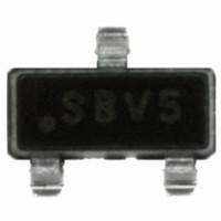
... Package Information 4.1 TLV4906K Package Outline VB1 Figure 7 Marking of the TLV4906K and distance of the chip to the upper side 3x0.4 0.95 Figure 8 PG-SC59-3-5 Package Outline Datasheet Year (y) = 0...9 Month (m) = 1... October n - November d - December 3 ±0.1 +0.05 -0.1 0 0.95 (0.55) 14 Package Information Branded Side d: Distance chip to upper side of IC ...
Page 15
... Reflow Soldering Figure 9 Footprint PG-SC59-3-5 (SOT23 compatible) Datasheet 0.8 1.2 15 Package Information 0.8 1.2 0.8 Wave Soldering Rev. 1.1, 2010-08-02 TLV4906K ...
Page 16
... Published by Infineon Technologies AG ...