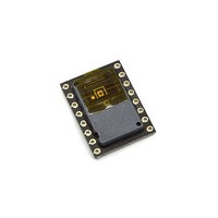
ADNS-3530 Avago Technologies US Inc., ADNS-3530 Datasheet - Page 11

ADNS-3530
Manufacturer Part Number
ADNS-3530
Description
Small Form Factor COB LED Sensor
Manufacturer
Avago Technologies US Inc.
Datasheet
1.ADNS-3530.pdf
(25 pages)
Specifications of ADNS-3530
Lead Free Status / RoHS Status
Lead free / RoHS Compliant
Lead Free Status / RoHS Status
Lead free / RoHS Compliant
Power Management Modes
The ADNS-3530 has three power-saving modes. Each
mode has a different motion detection period, affecting
response time to mouse motion (Response Time). The
sensor automatically changes to the appropriate mode,
depending on the time since the last reported motion
(Downshift Time). The parameters of each mode are
shown in the following table.
Mode
Rest 1
Rest 2
Rest 3
Motion Pin Timing
The motion pin is a level-sensitive output that signals
the microcontroller when motion has occurred. The mo-
tion pin is lowered whenever the motion bit is set; in
other words, whenever there is data in the Delta_X or
Delta_Y registers. Clearing the motion bit (by reading
Delta_Y and Delta_X, or writing to the Motion register)
will put the motion pin high.
LED Mode
For power savings, the LED will not be continuously on.
ADNS-3530 will flash the LED only when needed.
Synchronous Serial Port
The synchronous serial port is used to set and read pa-
rameters in the ADNS-3530, and to read out the motion
information.
The port is a four wire serial port. The host microcon-
troller always initiates communication; the ADNS-3530
never initiates data transfers. SCLK, MOSI, and NCS may
be driven directly by a microcontroller. The port pins
may be shared with other SPI slave devices. When the
NCS pin is high, the inputs are ignored and the output
is tri-stated.
11
Response Time
(Nominal)
16.5 ms
82 ms
410 ms
Downshift Time
(Nominal)
237 ms
8.4 s
504 s
The lines that comprise the SPI port:
Chip Select Operation
The serial port is activated after NCS goes low. If NCS
is raised during a transaction, the entire transaction is
aborted and the serial port will be reset. This is true for
all transactions. After a transaction is aborted, the nor-
mal address-to-data or transaction-to-transaction delay
is still required before beginning the next transaction.
To improve communication reliability, all serial transac-
tions should be framed by NCS. In other words, the port
should not remain enabled during periods of non-use
because ESD and EFT/B events could be interpreted as
serial communication and put the chip into an unknown
state. In addition, NCS must be raised after each burst-
mode transaction is complete to terminate burst-mode.
The port is not available for further use until burst-mode
is terminated.
Write Operation
Write operation, defined as data going from the micro-
controller to the ADNS-3530, is always initiated by the
microcontroller and consists of two bytes. The first byte
contains the address (seven bits) and has a “1” as its MSB
to indicate data direction. The second byte contains the
data. The ADNS-3530 reads MOSI on rising edges of
SCLK.
SCLK: Clock input. It is always generated by the mas-
MOSI: Input data. (Master Out/Slave In)
MISO: Output data. (Master In/Slave Out)
NCS:
Chip select input (active low). NCS needs to
ter (the microcontroller).
be low to activate the serial port; otherwise,
MISO will be high Z, and MOSI & SCLK will be
ignored. NCS can also be used to reset the se-
rial port in case of an error.


