AFBR-703SDDZ Avago Technologies US Inc., AFBR-703SDDZ Datasheet
AFBR-703SDDZ
Specifications of AFBR-703SDDZ


Related parts for AFBR-703SDDZ


AFBR-703SDDZ Summary of contents
Page 1
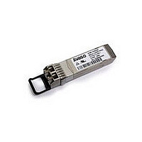
... Ethernet, 850nm SFP+ Transceiver Data Sheet Description The Avago AFBR-703SDDZ transceiver is part of a family of SFP+ products. This transceiver utilizes Avago’s 850nm VCSEL and PIN Detector technology to provide an IEEE 10Gb Ethernet design compliant with the 10GBASE-SR standard and allows the operation at 1.25GBd for Gigabit Ethernet application ...
Page 2
... For optical links, the ability to identify a fault at a local device, remote device or cable plant is crucial to speed- ing service of an installation. AFBR-703SDDZ real-time monitors of Tx_Bias, Tx_Power, Vcc, Temperature and Rx_ Power can be used to assess local transceiver current op- erating conditions ...
Page 3
... DC balanced. Transmit Disable (TX_DISABLE) The AFBR-703SDDZ accepts an LVTTL compatible trans- mit disable control signal input which shuts down the transmitter optical output. A high signal implements this function while a low signal allows normal transceiver operation ...
Page 4
... It may also result in improper operation and pos- sibly overstress the laser source. Performance degrada- tion or device failure may result. Connection of the AFBR-703SDDZ to a light source not compliant with IEEE Std. 802.3ae Clause 52 and SFF-8341 specifications, op- erating above maximum operating conditions manner inconsistent with it’ ...
Page 5
... Such conditions can be due to inputs from the host board (Vcc fluctuation, unbalanced code fault within the transceiver. US CDRH and EU TUV certificates are listed in table 1. Flammability The AFBR-703SDDZ optical transceiver is made of metal and high strength, heat resistant, chemical resistant and UL 94V-0 flame retardant plastic. ...
Page 6
Table 1. Regulatory Compliance Feature Test Method Electrostatic Discharge (ESD) MIL-STD-883C to the Electrical Contacts Method 3015.4 Electrostatic Discharge (ESD) IEC 61000-4-2 to the Duplex LC Receptacle Life Traffic ESD Immunity IEC 61000-4-2 Life Traffic ESD Immunity IEC 61000-4-2 Electromagnetic ...
Page 7
Tx_DISABLE Tx_FAULT SERDES IC PROTOCOL IC LOSS OF SIGNAL 4 kΩ MODULE DETECT SCL SDA Figure 2. Typical application configuration 0.1 μF 22 μ 0.1 μF 22 μF HOST BOARD SFP ...
Page 8
Table 2. Contact Description Contact Symbol Function/Description 1 VeeT Transmitter Signal Ground 2 TX_FAULT Transmitter Fault (LVTTL-O) – High indicates a fault condition 3 TX_DISABLE Transmitter Disable (LVTTL-I) – High or open disables the transmitter 4 SDA Two Wire Serial ...
Page 9
Table 3. Absolute Maximum Ratings Stress in excess of any of the individual Absolute Maximum Ratings can cause immediate catastrophic damage to the module even if all other parameters are within Recommended Operating Conditions. It should not be assumed that ...
Page 10
Table 5. Low Speed Signal Electrical Characteristics The following characteristics are defined over the Recommended Operating Conditions unless otherwise noted. Typical values are for Tc = 40°C. VccT and VccR = 3.3 V. Parameter Module Supply Current Power Dissipation TX_FAULT, ...
Page 11
NORMALIZED TIME (UNIT INTERVAL) Figure 5a. 10GBd Receiver Electrical Optical Eye Mask Definition Table 7. Two-Wire Interface Electrical Characteristics Parameter Symbol Host Vcc Range VccHTWI SCL and SDA ...
Page 12
Table 8a. 10GBd Optical Specifications - Transmitter The following characteristics are defined over the Recommended Operating Conditions unless otherwise noted. Typical values are for Tc = 40°C. VccT and VccR = 3.3 V. Parameter Laser OMA output power Laser mean ...
Page 13
Table 9a. 10GBd Optical Specifications - Receiver Parameter Stressed sensitivity (OMA) Receive sensitivity (OMA) Receive Power (P ) Overload ave Reflectance Center Wavelength RX_LOS (OMA) De-Asserted RX_LOS (OMA) Asserted RX_LOS (OMA) Hysteresis Vertical eye closure penalty Stressed eye jitter Electrical ...
Page 14
Table 10. 10 GBd Minimum Optical Modulation Amplitude Center RMS Spectral Width (nm) Wavelength Up to 0.05 to (nm) 0.05 0.1 840 to 842 -4.2 -4.2 842 to 844 -4.2 -4.2 844 to 846 -4.2 -4.2 846 to 848 -4.3 ...
Page 15
Table 12. Control Functions: Two-Wire Interface Timing Characteristics The following characteristics are defined over the Recommended Operating Conditions unless otherwise noted. Parameter TX_DISABLE Assert Time TX_DISABLE Negate Time TX_FAULT Assert Time Rx_LOS Assert Time Rx_LOS Deassert Time Analog parameter data ...
Page 16
Table 13. Transceiver Digital Diagnostic Monitor (Real Time Sense) Characteristics The following characteristics are defined over the Recommended Operating Conditions unless otherwise noted. Typical values are for Tc = 40°C. VccT and VccR = 3.3 V. Parameter Transceiver Internal Temperature ...
Page 17
... Addresses 63 and 95 are checksums calculated (per SFF-8472) and stored prior to product shipment. 4. Addresses 68-83 specify the AFBR-703SDDZ ASCII serial number and will vary on a per unit basis. 5. Addresses 84-91 specify the AFBR-703SDDZ ASCII date code and will vary on a per date code basis. 17 ...
Page 18
... Transmitted average optical power (Tx Pwr) is decoded bit unsigned integer in increments of 0.1 PW. 5. Received average optical power (Rx Pwr) is decoded bit unsigned integer in increments of 0.1 PW. 6. Bytes 56-94 are not intended for use with AFBR-703SDDZ, but have been set to default values per SFF-8472. 7. Byte checksum calculated (per SFF-8472) and stored prior to product shipment. ...
Page 19
... Data Ready (Bar) Indicates transceiver is powered and real time sense data is ready Ready) Notes: 1. The response time for soft commands of the AFBR-703SDDZ is 100 msec as specified by SFF-8472. 2. Bit 6 is logic OR’d with the SFP TX_DISABLE input on contact 3; either asserted will disable the SFP+ transmitter. 19 Description Read/write bit that allows software Tx rate control ...
Page 20
Table 18. EEPROM Serial ID Memory Contents – Alarms and Warnings (Address A2h, Bytes 112, 113, 116, 117) Byte Bit Flag Bit Name Description 112 7 Temp High Alarm 6 Temp Low Alarm 5 Vcc High Alarm 4 Vcc Low ...
Page 21
TCASE REFERENCE POINT LATCHCOLOR BLACK 6. Figure 7. Module Drawing Figure 8. Module label 21 13.6 13.7 0.94 UNCOMPRESSED 12.3 0.65 UNCOMPRESSED 15.1 UNCOMPRESSED 47.5 13.2 ±0.1 8.6 ±0.1 ...
Page 22
Appendix: Rate Select Control RX and TX rates can be independently controlled by either hardware input pins or via register writes. Module electri- cal input pins 7 and 9 are used to select RX and TX rate respectively. Status of ...