AFBR-703SDDZ Avago Technologies US Inc., AFBR-703SDDZ Datasheet - Page 3
AFBR-703SDDZ
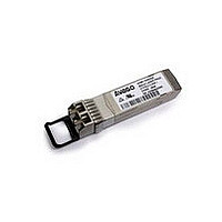
Manufacturer Part Number
AFBR-703SDDZ
Description
SFP+ 850nm 1/10GbE SR MMF,Gen2 STD
Manufacturer
Avago Technologies US Inc.
Series
-r
Datasheet
1.AFBR-703SDDZ.pdf
(22 pages)
Specifications of AFBR-703SDDZ
Data Rate
10.312Gbd
Wavelength
850nm
Applications
Ethernet
Voltage - Supply
3.135 V ~ 3.465 V
Connector Type
LC Duplex
Mounting Type
SFP+
Optical Fiber Type
TX/RX
Data Transfer Rate
10313MBd
Optical Rise Time
0.028ns
Optical Fall Time
0.028ns
Operating Temperature Classification
Commercial
Peak Wavelength
860nm
Package Type
SFP
Operating Supply Voltage (min)
3.135V
Operating Supply Voltage (typ)
3.3V
Operating Supply Voltage (max)
3.465V
Output Current
20mA
Operating Temp Range
0C to 70C
Mounting
Snap Fit To Panel
Pin Count
20
Lead Free Status / RoHS Status
Lead free / RoHS Compliant
Lead Free Status / RoHS Status
Lead free / RoHS Compliant


Transmitter Section
The transmitter section includes the Transmitter
Optical Sub-Assembly (TOSA) and laser driver circuitry.
The TOSA, containing an Avago designed and manufac-
tured 850 nm VCSEL (Vertical Cavity Surface Emitting
Laser) light source, is located at the optical interface and
mates with the LC optical connector. The TOSA is driven
by an IC which uses the incoming differential high speed
logic signal to modulate the laser diode driver current.
This Tx laser driver circuit regulates the optical power at
a constant level provided the incoming data pattern is
DC balanced.
Transmit Disable (TX_DISABLE)
The AFBR-703SDDZ accepts an LVTTL compatible trans-
mit disable control signal input which shuts down the
transmitter optical output. A high signal implements this
function while a low signal allows normal transceiver
operation. In the event of a fault (e.g. eye safety circuit
activated), cycling this control signal resets the module
as depicted in Figure 6. An internal pull up resistor dis-
ables the transceiver transmitter until the host pulls the
input low. TX_DISABLE can also be asserted via the two-
wire interface (address A2h, byte 110, bit 6) and moni-
tored (address A2h, byte 110, bit 7).
The contents of A2h, byte 110, bit 6 are logic OR’d with
hardware TX_DISABLE (contact 3) to control transmitter
operation.
Figure 1. Transceiver functional diagram
3
OPTICAL INTERFACE
LIGHT FROM FIBER
LIGHT TO FIBER
RECEIVER
TRANSMITTER
PHOTO-DETECTOR
VCSEL
CONTROLLER & MEMORY
AMPLIFICATION
& QUANTIZATION
Transmit Fault (TX_FAULT)
A catastrophic laser fault will activate the transmitter
signal, TX_FAULT, and disable the laser. This signal is
an open collector output (pull-up required on the host
board). A low signal indicates normal laser operation
and a high signal indicates a fault. The TX_FAULT will
be latched high when a laser fault occurs and is cleared
by toggling the TX_DISABLE input or power cycling the
transceiver. The transmitter fault condition can also be
monitored via the two-wire serial interface (address A2,
byte 110, bit 2).
CIRCUITRY
DRIVER &
SAFETY
LASER
RD+ (RECEIVE DATA)
RD– (RECEIVE DATA)
RX_LOS
RS0
RS1
SDA
SCL
MOD-ABS
TX_DISABLE
TD+ (TRANSMIT DATA)
TD– (TRANSMIT DATA)
TX_FAULT
ELECTRICAL INTERFACE
Related parts for AFBR-703SDDZ
Image
Part Number
Description
Manufacturer
Datasheet
Request
R

Part Number:
Description:
TXRX ETHERNET 125MBD MMF 2X5
Manufacturer:
Avago Technologies US Inc.
Datasheet:

Part Number:
Description:
TXRX OPT XFP 10GB/S 850NM
Manufacturer:
Avago Technologies US Inc.
Datasheet:

Part Number:
Description:
TXRX OPT 1X9 100MBPS DUPLEX SC
Manufacturer:
Avago Technologies US Inc.
Datasheet:

Part Number:
Description:
TXRX OPT 1X9 100MBPS DUPLEX ST
Manufacturer:
Avago Technologies US Inc.
Datasheet:

Part Number:
Description:
TXRX OPT 1X9 100MBPS DUPL ST SIP
Manufacturer:
Avago Technologies US Inc.
Datasheet:

Part Number:
Description:
TXRX OPT 1X9 100MBPS DUPL SC SIP
Manufacturer:
Avago Technologies US Inc.
Datasheet:

Part Number:
Description:
TXRX OPT 1X9 100MBPS DUPL ST SIP
Manufacturer:
Avago Technologies US Inc.
Datasheet:

Part Number:
Description:
TXRX ATM SONET OC3 3V SC 1X9
Manufacturer:
Avago Technologies US Inc.
Datasheet:
Part Number:
Description:
TXRX ATM/SONET OC-3 2X5
Manufacturer:
Avago Technologies US Inc.
Datasheet:

Part Number:
Description:
TXRX 127MBD DUPLEX SC 1X9
Manufacturer:
Avago Technologies US Inc.
Datasheet:

Part Number:
Description:
OPTOCOUPLER GATE DRV 2A 16-SOIC
Manufacturer:
Avago Technologies US Inc.
Datasheet:
Part Number:
Description:
OPTOCOUPLER 2CH 2.5A 16-SOIC
Manufacturer:
Avago Technologies US Inc.
Datasheet:

Part Number:
Description:
OPTOCOUPLER GATE DRV 0.4A 16SOIC
Manufacturer:
Avago Technologies US Inc.
Datasheet:

Part Number:
Description:
OPTOCOUPLER 2.0A 250KHZ 8-DIP
Manufacturer:
Avago Technologies US Inc.
Datasheet:

Part Number:
Description:
OPTOCOUPLER 2.0A 250KHZ GW 8-SMD
Manufacturer:
Avago Technologies US Inc.
Datasheet: