FM-RX1-433A RF Solutions, FM-RX1-433A Datasheet - Page 3
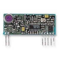
FM-RX1-433A
Manufacturer Part Number
FM-RX1-433A
Description
MODULE, RECEIVER, FM
Manufacturer
RF Solutions
Datasheet
1.FM-RX1-433A.pdf
(7 pages)
Specifications of FM-RX1-433A
Svhc
No SVHC (15-Dec-2010)
Current Rating
14mA
Data Rate Max
10000bps
Frequency
433MHz
Operating Distance
300m
Operating Temperature Max
55°C
Operating Temperature Min
-10°C
Safety Category
DTI MPT1340


DS000021
This output of the module may be used in several ways:-
This is a CMOS compatible data output, normally used to drive a digital decoder IC or a microprocessor
performing the data decoding. The data slicer in the receive module is designed to accept data with a wide range
of pulse widths and mark-space ratio’s. See specification table for limiting values.
The data slicer has a 10ms transient response time. This is the settling time of the adaptive comparator, i.e. the
first 10ms of signal may be corrupt at the data output.
This is the FM demodulator’s output after buffering and filtering. Since it is taken before the data slicer in the
module, it may be used to drive external data slicers/demodulator’s in cases where the internal data slicer is not
suitable. This is the case where an analogue subcarrier is being employed, e.g. 2-tone AFSK or DTMF tones. In
these cases the AF output is used to drive the FSK/DTMF decoder directly. The AF output is also a very useful
test point for monitoring signals or interference. The AF output is DC coupled to the FM demodulator, thus the DC
level varies with the frequency of the incoming signal.
The positioning of the antenna is of the utmost importance and is an important factor in the determining system
range, the following notes should assist in obtaining optimum performance:-
Keep it clear of other metal in the system. This applies particularly to the ‘hot’ (top) end of the antenna. The best
position by far is sticking out of the top of the product, but if this is not possible for practical or ergonomic
reasons a compromise may be needed. If an internal antenna must be used, try to keep it away from other metal
components, particularly larger components such as transformers, batteries and PCB tracks or the earth plane.
The space around the antenna is as important as the antenna itself.
Keep the antenna away from interference sources. Bad interference can easily reduce system range by a factor
of 5. High speed logic is one of the worst sources; fast logic edges have harmonics which extend into the UHF
band, and PCB tracks can radiate these harmonics most efficiently. Single chip microcontrollers and ground
planed logic boards reduce this problem significantly.
For more detail information on antenna design, please see RF Solutions product catalogue.
DETECT OUTPUT (Pin 3)
INTERNAL DATA SLICER (Pin 7)
A.F. OUTPUT (Pin 6)
SUPPLY REQUIREMENTS
The module requires a clean supply. Noise and ‘hash’ in the 5 to 500 kHz band and 16MHz +/- 1MHz must be
<2mV. We recommend a 10 F capacitor and 10
supply is in doubt.
ANTENNA DESIGN
1. Connecting to Vcc (pin 5) with a 47k
2. Pulled down to 0 volts with a 47K
3. To drive the base of a PNP transistor (see Test Circuit) to derive a logic compatible carrier detect.
4. For duty cycle power saving control where battery life needs to be maximised (e.g. in portable equipment).
Rev 2.1
By pulsing the decoder on/off the average supply current may often be reduced by a factor of 20 or more,
depending on the system requirements. The data detect output is valid 1.5ms (2.5ms worst case) after
application of the supply, and is used to inhibit the power saving while data decoding is being completed.
Jul ‘99
FM R. F. R
1999 REG No 277 4001, ENGLAND.
mutes the AF and DATA outputs (both go to 0 volts).
ECEIVER
resistor unmutes the AF and DATA outputs for normal operation.
series feed resistor in cases where the cleanness of the
M
ODULES
.
FMRX1- XXXX
Page 3
Related parts for FM-RX1-433A
Image
Part Number
Description
Manufacturer
Datasheet
Request
R

Part Number:
Description:
RECEIVER, HYBRID, FM
Manufacturer:
TELECONTROLLI
Datasheet:
Part Number:
Description:
TRANSMITTER, HYBRID, FM
Manufacturer:
TELECONTROLLI
Datasheet:

Part Number:
Description:
RECEIVER, FM
Manufacturer:
RF Solutions
Datasheet:

Part Number:
Description:
MODULE, TRANSMITTER, FM
Manufacturer:
RF Solutions
Datasheet:
Part Number:
Description:
FM / Fmx-r Stereo Decoders
Manufacturer:
ETC
Datasheet:

Part Number:
Description:
IC ENCODER TRANSMITTER RF 8DIP
Manufacturer:
RF Solutions
Datasheet:

Part Number:
Description:
IC DECODER RECEIVER RF 18DIP
Manufacturer:
RF Solutions
Datasheet:

Part Number:
Description:
IC ENCODER 3 DGTL I/O SOT23-6
Manufacturer:
RF Solutions
Datasheet:

Part Number:
Description:
IC ENCODER 3 DGTL I/O 8-PDIP
Manufacturer:
RF Solutions
Datasheet:

Part Number:
Description:
IC DECODER 3 DGTL I/O 8-PDIP
Manufacturer:
RF Solutions
Datasheet:

Part Number:
Description:
IC DECODER 3 DGTL I/O 8-SOIC
Manufacturer:
RF Solutions
Datasheet:
Part Number:
Description:
118 SERIES AM REMOTE CONTROL SYSTEMS.
Manufacturer:
RF Solutions Ltd.