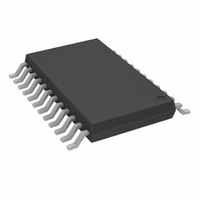
AD5440YRUZ Analog Devices Inc, AD5440YRUZ Datasheet - Page 16

AD5440YRUZ
Manufacturer Part Number
AD5440YRUZ
Description
IC,D/A CONVERTER,DUAL,10-BIT,CMOS,TSSOP,24PIN
Manufacturer
Analog Devices Inc
Datasheet
1.AD5428YRUZ.pdf
(32 pages)
Specifications of AD5440YRUZ
Settling Time
35ns
Number Of Bits
10
Data Interface
Parallel
Number Of Converters
2
Voltage Supply Source
Single Supply
Power Dissipation (max)
3.3µW
Operating Temperature
-40°C ~ 125°C
Mounting Type
Surface Mount
Package / Case
24-TSSOP
Number Of Channels
2
Resolution
10b
Conversion Rate
21.3MSPS
Interface Type
Parallel
Single Supply Voltage (typ)
3.3/5V
Dual Supply Voltage (typ)
Not RequiredV
Architecture
R-2R
Power Supply Requirement
Single
Output Type
Current
Integral Nonlinearity Error
±0.5+/- LSB
Single Supply Voltage (min)
2.5V
Single Supply Voltage (max)
5.5V
Dual Supply Voltage (min)
Not RequiredV
Dual Supply Voltage (max)
Not RequiredV
Operating Temp Range
-40C to 125C
Operating Temperature Classification
Automotive
Mounting
Surface Mount
Pin Count
24
Package Type
TSSOP
Lead Free Status / RoHS Status
Lead free / RoHS Compliant
For Use With
EVAL-AD5440EBZ - BOARD EVAL FOR AD5440
Lead Free Status / Rohs Status
Compliant
Available stocks
Company
Part Number
Manufacturer
Quantity
Price
Company:
Part Number:
AD5440YRUZ
Manufacturer:
Analog Devices Inc
Quantity:
135
Part Number:
AD5440YRUZ
Manufacturer:
ADI/亚德诺
Quantity:
20 000
AD5428/AD5440/AD5447
GENERAL DESCRIPTION
DAC SECTION
The AD5428/AD5440/AD5447 are CMOS 8-, 10-, and 12-bit,
dual-channel, current output DACs consisting of a standard
inverting R-2R ladder configuration. Figure 37 shows a simplified
diagram for a single channel of the 8-bit AD5428. The feedback
resistor R
(with a minimum of 8 kΩ and a maximum of 12 kΩ). If I
and AGND are kept at the same potential, a constant current
flows into each ladder leg, regardless of digital input code.
Therefore, the input resistance presented at V
constant and nominally of value R. The DAC output (I
code-dependent, producing various resistances and
capacitances. When choosing an external amplifier, take into
account the variation in impedance generated by the DAC on
the amplifier’s inverting input node.
Access is provided to the V
and DAC B, making the devices extremely versatile and
allowing them to be configured in several operating modes,
such as unipolar output mode, 4-quadrant multiplication
bipolar mode, or single-supply mode. Note that a matching
switch is used in series with the internal R
If users attempt to measure R
to achieve continuity.
V
REF
FB
A has a value of R. The value of R is typically 10 kΩ
S1
2R
DAC DATA LATCHES
R
AND DRIVERS
Figure 37. Simplified Ladder
S2
2R
R
REF
2R
S3
FB
, R
R
A, power must be applied to V
FB
, and I
S8
2R
2R
OUT
FB
R
A feedback resistor.
terminals of DAC A
REF
R
I
AGND
OUT
A is always
FB
A
A
OUT
OUT
) is
1
Rev. B | Page 16 of 32
DD
CIRCUIT OPERATION
Unipolar Mode
Using a single op amp, these devices can easily be configured to
provide 2-quadrant multiplying operation or a unipolar output
voltage swing, as shown in Figure 38. When an output amplifier
is connected in unipolar mode, the output voltage is given by
where:
D is the fractional representation of the digital word loaded to
the DAC.
n is the resolution of the DAC.
Note that the output voltage polarity is opposite to the V
polarity for dc reference voltages. These DACs are designed to
operate with either negative or positive reference voltages. The
V
the on and off states of the DAC switches.
These DACs are also designed to accommodate ac reference
input signals in the range of –10 V to +10 V.
With a fixed 10 V reference, the circuit in Figure 38 gives a
unipolar 0 V to –10 V output voltage swing. When V
signal, the circuit performs 2-quadrant multiplication.
Table 7 shows the relationship between digital code and the
expected output voltage for unipolar operation using the 8-bit
AD5428.
Table 7. Unipolar Code
Digital Input
1111 1111
1000 0000
0000 0001
0000 0000
DD
D = 0 to 255 (8-bit AD5428)
= 0 to 1023 (10-bit AD5440)
= 0 to 4095 (12-bit AD5447)
power pin is only used by the internal digital logic to drive
V
OUT
=
−
V
REF
×
D
Analog Output (V)
–V
–V
–V
–V
2 /
REF
REF
REF
REF
n
(128/256) = –V
(255/256)
(1/256)
(0/256) = 0
REF
/2
IN
is an ac
REF


