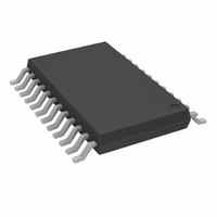
AD5440YRUZ Analog Devices Inc, AD5440YRUZ Datasheet - Page 8

AD5440YRUZ
Manufacturer Part Number
AD5440YRUZ
Description
IC,D/A CONVERTER,DUAL,10-BIT,CMOS,TSSOP,24PIN
Manufacturer
Analog Devices Inc
Datasheet
1.AD5428YRUZ.pdf
(32 pages)
Specifications of AD5440YRUZ
Settling Time
35ns
Number Of Bits
10
Data Interface
Parallel
Number Of Converters
2
Voltage Supply Source
Single Supply
Power Dissipation (max)
3.3µW
Operating Temperature
-40°C ~ 125°C
Mounting Type
Surface Mount
Package / Case
24-TSSOP
Number Of Channels
2
Resolution
10b
Conversion Rate
21.3MSPS
Interface Type
Parallel
Single Supply Voltage (typ)
3.3/5V
Dual Supply Voltage (typ)
Not RequiredV
Architecture
R-2R
Power Supply Requirement
Single
Output Type
Current
Integral Nonlinearity Error
±0.5+/- LSB
Single Supply Voltage (min)
2.5V
Single Supply Voltage (max)
5.5V
Dual Supply Voltage (min)
Not RequiredV
Dual Supply Voltage (max)
Not RequiredV
Operating Temp Range
-40C to 125C
Operating Temperature Classification
Automotive
Mounting
Surface Mount
Pin Count
24
Package Type
TSSOP
Lead Free Status / RoHS Status
Lead free / RoHS Compliant
For Use With
EVAL-AD5440EBZ - BOARD EVAL FOR AD5440
Lead Free Status / Rohs Status
Compliant
Available stocks
Company
Part Number
Manufacturer
Quantity
Price
Company:
Part Number:
AD5440YRUZ
Manufacturer:
Analog Devices Inc
Quantity:
135
Part Number:
AD5440YRUZ
Manufacturer:
ADI/亚德诺
Quantity:
20 000
AD5428/AD5440/AD5447
Table 5. AD5440 Pin Function Descriptions
Pin No.
1
2, 24
3, 23
4, 22
5
6
7 to16
19
20
21
Mnemonic
AGND
I
R
V
DGND
DAC A/B
DB9 to DB0
CS
R/W
V
OUT
FB
REF
DD
A, R
A, I
A, V
OUT
FB
REF
B
B
B
Function
DAC Ground Pin. This pin should typically be tied to the analog ground of the system, but can be biased to
achieve single-supply operation.
DAC Current Outputs.
DAC Feedback Resistor Pins. Establish voltage output for the DAC by connecting to an external amplifier
output.
DAC Reference Voltage Input Terminals.
Digital Ground Pin.
Selects DAC A or DAC B. Low selects DAC A; high selects DAC B.
Parallel Data Bits 9 Through 0.
Chip Select Input. Active low. Used in conjunction with R/W to load parallel data to the input latch or to read
data from the DAC register.
Read/Write. When low, used in conjunction with CS to load parallel data. When high, used in conjunction with
CS to read back contents of the DAC register.
Positive Power Supply Input. This part can be operated from a supply of 2.5 V to 5.5 V.
Figure 5. Pin Configuration 24-Lead TSSOP (RU-24)
DAC A/B
V
AGND
DGND
I
OUT
R
REF
DB9
DB8
DB7
DB6
DB5
DB4
FB
A
A
A
10
11
12
1
2
3
4
5
6
7
8
9
NC = NO CONNECT
Rev. B | Page 8 of 32
(Not to Scale)
AD5440
TOP VIEW
24
23
22
21
20
19
18
17
16
15
14
13
I
R
V
V
R/W
CS
NC
NC
DB0 (LSB)
DB1
DB2
DB3
OUT
REF
DD
FB
B
B
B


