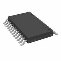
AD5440YRUZ Analog Devices Inc, AD5440YRUZ Datasheet - Page 19

AD5440YRUZ
Manufacturer Part Number
AD5440YRUZ
Description
IC,D/A CONVERTER,DUAL,10-BIT,CMOS,TSSOP,24PIN
Manufacturer
Analog Devices Inc
Datasheet
1.AD5428YRUZ.pdf
(32 pages)
Specifications of AD5440YRUZ
Settling Time
35ns
Number Of Bits
10
Data Interface
Parallel
Number Of Converters
2
Voltage Supply Source
Single Supply
Power Dissipation (max)
3.3µW
Operating Temperature
-40°C ~ 125°C
Mounting Type
Surface Mount
Package / Case
24-TSSOP
Number Of Channels
2
Resolution
10b
Conversion Rate
21.3MSPS
Interface Type
Parallel
Single Supply Voltage (typ)
3.3/5V
Dual Supply Voltage (typ)
Not RequiredV
Architecture
R-2R
Power Supply Requirement
Single
Output Type
Current
Integral Nonlinearity Error
±0.5+/- LSB
Single Supply Voltage (min)
2.5V
Single Supply Voltage (max)
5.5V
Dual Supply Voltage (min)
Not RequiredV
Dual Supply Voltage (max)
Not RequiredV
Operating Temp Range
-40C to 125C
Operating Temperature Classification
Automotive
Mounting
Surface Mount
Pin Count
24
Package Type
TSSOP
Lead Free Status / RoHS Status
Lead free / RoHS Compliant
For Use With
EVAL-AD5440EBZ - BOARD EVAL FOR AD5440
Lead Free Status / Rohs Status
Compliant
Available stocks
Company
Part Number
Manufacturer
Quantity
Price
Company:
Part Number:
AD5440YRUZ
Manufacturer:
Analog Devices Inc
Quantity:
135
Part Number:
AD5440YRUZ
Manufacturer:
ADI/亚德诺
Quantity:
20 000
SINGLE-SUPPLY APPLICATIONS
Voltage-Switching Mode
Figure 40 shows the DACs operating in voltage-switching
mode. The reference voltage, V
and the output voltage is available at the V
configuration, a positive reference voltage results in a positive
output voltage, making single-supply operation possible. The
output from the DAC is voltage at constant impedance (the
DAC ladder resistance). Therefore, an op amp is necessary to
buffer the output voltage. The reference input no longer sees
constant input impedance, but one that varies with code.
Therefore, the voltage input should be driven from a low
impedance source.
Note that V
the DAC ladder no longer have the same source-drain drive
voltage. As a result, their on resistance differs and degrades the
integral linearity of the DAC. Also, V
more than 0.3 V, or an internal diode turns on, causing the
device to exceed the maximum ratings. In this type of
application, the full range of multiplying capability of the DAC
is lost.
Positive Output Voltage
The output voltage polarity is opposite to the V
dc reference voltages. To achieve a positive voltage output, an
applied negative reference to the input of the DAC is preferred
over the output inversion through an inverting amplifier
because of the resistor’s tolerance errors. To generate a negative
reference, the reference can be level-shifted by an op amp such
that the V
ground and –2.5 V, respectively, as shown in Figure 41.
V
IN
NOTES
1. ADDITIONAL PINS OMITTED FOR CLARITY.
2. C1 PHASE COMPENSATION (1pF TO 2pF) MAY BE REQUIRED
OUT
IF A1 IS A HIGH SPEED AMPLIFIER.
Figure 40. Single-Supply Voltage-Switching Mode
IN
I
AGND
OUT
and GND pins of the reference become the virtual
is limited to low voltages because the switches in
A
R
FB
A
GND
V
V
DD
DD
V
REF
IN
A
, is applied to the I
R1
IN
must not go negative by
REF
A terminal. In this
R2
REF
polarity for
OUT
V
A pin,
OUT
Rev. B | Page 19 of 32
ADDING GAIN
In applications where the output voltage must be greater than
V
it can be achieved in a single stage. Consider the effect of temper-
ature coefficients of the thin film resistors of the DAC. Simply
placing a resistor in series with the R
in the temperature coefficients, resulting in larger gain temper-
ature coefficient errors. Instead, the circuit in Figure 42 shows
the recommended method for increasing the gain of the circuit.
R1, R2, and R3 should have similar temperature coefficients,
but they need not match the temperature coefficients of the
DAC. This approach is recommended in circuits where gains of
greater than 1 are required.
NOTES
1. ADDITIONAL PINS OMITTED FOR CLARITY.
2. C1 PHASE COMPENSATION (1pF TO 2pF) MAY BE REQUIRED
V
NOTES
1. ADDITIONAL PINS OMITTED FOR CLARITY.
2. C1 PHASE COMPENSATION (1pF TO 2pF) MAY BE REQUIRED
IN
IN
IF A1 IS A HIGH SPEED AMPLIFIER.
IF A1 IS A HIGH SPEED AMPLIFIER.
, gain can be added with an additional external amplifier, or
R1
Figure 41. Positive Voltage Output with Minimum Components
+5V
–5V
–2.5V
V
V
Figure 42. Increasing Gain of Current Output DAC
REF
ADR03
OUT
GND
8-/10-/12-BIT
A
V
V
V
GND
IN
DAC
DD
DD
V
REF
8-/10-/12-BIT
A
V
R
DD
I
AGND
AD5428/AD5440/AD5447
FB
GND
OUT
V
DAC
DD
= 5V
A
A
R
I
AGND
FB
FB
OUT
C1
A
resistor causes mismatches
A
R3
R2
C1
GAIN =
R
1
=
R2
R2R3
V
0V to 2.5V
OUT
R2 + R3
V
+
OUT
R3
R2
=


