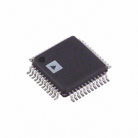
AD7724ASTZ-REEL Analog Devices Inc, AD7724ASTZ-REEL Datasheet - Page 6

AD7724ASTZ-REEL
Manufacturer Part Number
AD7724ASTZ-REEL
Description
FOUR CHANNEL SIGMA DELTA MODULATOR I.C.
Manufacturer
Analog Devices Inc
Type
Modulatorr
Datasheet
1.AD7724ASTZ-REEL.pdf
(16 pages)
Specifications of AD7724ASTZ-REEL
Resolution (bits)
15 b
Sampling Rate (per Second)
250k
Data Interface
Serial
Voltage Supply Source
Analog and Digital
Voltage - Supply
2.85 V ~ 5.25 V
Operating Temperature
-40°C ~ 85°C
Mounting Type
Surface Mount
Package / Case
48-LQFP
Lead Free Status / RoHS Status
Lead free / RoHS Compliant
Available stocks
Company
Part Number
Manufacturer
Quantity
Price
Company:
Part Number:
AD7724ASTZ-REEL
Manufacturer:
TDK
Quantity:
460 000
Company:
Part Number:
AD7724ASTZ-REEL
Manufacturer:
Analog Devices Inc
Quantity:
10 000
AD7724
Mnemonic
AVDD
AGND
AVIN(–), AVIN(+) Analog Input to Modulator A. In unipolar operation, the analog input range on AVIN(+) is AVIN(–) to
STBY
MZERO
RESET
XTAL1
XTAL2/MCLK
DVDD
DGND
ADATA
BDATA
SCLK
DVDD1
DVAL
XTAL_OFF
BIP
GC
BVIN(–), BVIN(+) Analog Input to Modulator B. In unipolar operation, the analog input range on BVIN(+) is BVIN(–) to
REF2B
REF1
REF2A
Clock Input. An external clock source can be applied directly to this pin with XTAL_OFF tied high. In this
Description
Analog Positive Supply Voltage, 5 V ± 5%.
Ground reference point for analog circuitry.
(AVIN(–) + VREF); for bipolar operation, the analog input range on AVIN(+) is (AVIN(–) ± VREF/2). The
absolute analog input range must lie between 0 and AVDD. The input range is continuously sampled and pro-
cessed by the analog modulator.
Standby, Logic Input. When STBY is high, the device is placed in a low power mode. When STBY is low, the
device is powered up.
Digital Control Input. When MZERO is high, the modulator inputs are internally grounded i.e. tied to AGND
in unipolar mode and REF2 in bipolar mode. MZERO allows on-chip offsets to be calibrated out. MZERO is
low for normal operation.
Reset Logic Input. RESET is an asynchronous input. When RESET is taken high, the sigma-delta modulator is
reset by shorting the integrator capacitors in the modulator. DVAL goes low for 20 MCLK cycles while the
modulator is being reset.
Input to Crystal Oscillator Amplifier. This pin can also be used to gain up a small input square or sine wave
with XTAL_OFF tied low (see Figure 32 on page 12). When a clock source is applied to XTAL1, SCLK will
be inverted and the XTAL1_CLK to SCLK delay will be typically 14 ns longer than t
case, XTAL1 should be tied to AGND. Alternatively, a parallel resonant fundamental frequency crystal, in
parallel with a 1 MΩ resistor, can be connected between XTAL1 and XTAL2 with XTAL_OFF tied low. Exter-
nal capacitors are then required from the XTAL1 and XTAL2 pins to ground. Consult the crystal
manufacturer's recommendation for the load capacitors.
A sine wave can also be used to provide the clock. A sine wave with a voltage swing between 0.4 V p-p and
4 V p-p is needed. XTAL_OFF is tied low and a 1 MΩ resistor is needed between XTAL1 and XTAL2. A
22 pF capacitor is connected in parallel with this resistor. The sine wave is ac coupled to XTAL1 using a
120 pF capacitor. The use of a sine wave to generate the clock eliminates the need for a square wave clock
source which introduces noise.
Digital Supply Voltage, 5 V ± 5%.
Ground reference for the digital circuitry.
Modulator A Bit Stream. The digital bit stream from the sigma-delta modulator is output at ADATA.
Modulator B Bit Stream. The digital bit stream from the sigma-delta modulator is output at BDATA.
Serial Clock, Logic Output. The bit stream from modulator A and modulator B is valid on the rising edge of
ASCLK.
Digital Supply Voltage for the digital outputs. DVDD1 can have a value of 5 V ± 5% or 3 V ± 5% so that the
logic outputs can be 3 V or 5 V compatible.
Data Valid Logic Output. A logic high on DVAL indicates that the data bit stream from the AD7724 is an
accurate digital representation of the analog voltage at the input to the sigma-delta modulator. The DVAL pin
is set low for 20 MCLK cycles if the analog input is overranged.
Oscillator Enable Input. A logic high disables the crystal oscillator amplifier to allow use of an external clock
source. XTAL_OFF is set to a logic low when an external crystal is used between XTAL1 and XTAL2.
Analog Input Range Select, Logic Input. A logic low on this input selects unipolar mode. A logic high selects
bipolar mode.
Digital Control Input. When GC is high, the gain error of the modulator can be calibrated.
(BVIN(–) + VREF); for bipolar operation, the analog input range on BVIN(+) is (BVIN(–) ± VREF/2). The
absolute analog input range must lie between 0 and AVDD. The input range is continuously sampled and pro-
cessed by the analog modulator.
Reference Input/Output to Sigma-Delta Modulator B. REF2B connects to the output of an external buffer amplifier
used to drive sigma-delta modulator B. When REF2B is used as an input, REF1 must be connected to AGND.
Reference Input/Output. REF1 connects through 3 kΩ to the output of the internal 2.5 V reference and to the
input of two buffer amplifiers that drive Σ-∆ modulator A and Σ-∆ modulator B. The pin can be overdriven with
an external 2.5 V reference.
Reference Input/Output to Sigma-Delta Modulator A. REF2A connects to the output of an external buffer
amplifier used to drive sigma-delta modulator A. When REF2A is used as an input, REF1 must be connected
to AGND.
PIN FUNCTION DESCRIPTIONS
DELAY
.


