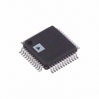
AD7724ASTZ-REEL Analog Devices Inc, AD7724ASTZ-REEL Datasheet - Page 7

AD7724ASTZ-REEL
Manufacturer Part Number
AD7724ASTZ-REEL
Description
FOUR CHANNEL SIGMA DELTA MODULATOR I.C.
Manufacturer
Analog Devices Inc
Type
Modulatorr
Datasheet
1.AD7724ASTZ-REEL.pdf
(16 pages)
Specifications of AD7724ASTZ-REEL
Resolution (bits)
15 b
Sampling Rate (per Second)
250k
Data Interface
Serial
Voltage Supply Source
Analog and Digital
Voltage - Supply
2.85 V ~ 5.25 V
Operating Temperature
-40°C ~ 85°C
Mounting Type
Surface Mount
Package / Case
48-LQFP
Lead Free Status / RoHS Status
Lead free / RoHS Compliant
Available stocks
Company
Part Number
Manufacturer
Quantity
Price
Company:
Part Number:
AD7724ASTZ-REEL
Manufacturer:
TDK
Quantity:
460 000
Company:
Part Number:
AD7724ASTZ-REEL
Manufacturer:
Analog Devices Inc
Quantity:
10 000
TERMINOLOGY (IDEAL FIR FILTER USED WITH AD7724
[FIGURE 1])
Integral Nonlinearity
This is the maximum deviation of any code from a straight line
passing through the endpoints of the transfer function. The
endpoints of the transfer function are zero scale (not to be con-
fused with bipolar zero), a point 0.5 LSB below the first code
transition (100 . . . 00 to 100 . . . 01 in bipolar mode and
000 . . . 00 to 000 . . . 01 in unipolar mode) and full scale, a
point 0.5 LSB above the last code transition (011 . . . 10 to
011 . . . 11 in bipolar mode and 111 . . . 10 to 111 . . . 11 in
unipolar mode). The error is expressed in LSBs.
Common-Mode Rejection Ratio
The ability of a device to reject the effect of a voltage applied to
both input terminals simultaneously—often through variation of
a ground level—is specified as a common–mode rejection ratio.
CMRR is the ratio of gain for the differential signal to the gain
for the common-mode signal.
Unipolar Offset Error
Unipolar offset error is the deviation of the first code transition
from the ideal VIN(+) voltage which is (VIN(–) + 0.5 LSB)
when operating in the unipolar mode.
Bipolar Offset Error
This is the deviation of the midscale transition (111 . . . 11
to 000 . . . 00) from the ideal VIN(+) voltage which is (VIN(–)
–0.5 LSB) when operating in the bipolar mode.
Gain Error
The first code transition should occur at an analog value 1/2 LSB
above minus full scale. The last code transition should occur for
an analog value 1 1/2 LSB below the nominal full-scale. Gain
error is the deviation of the actual difference between first and
last code transitions and the ideal difference between first and
last code transitions.
Signal-to-(Noise + Distortion)
Signal-to-(Noise + Distortion) is the measured signal-to-noise
plus distortion ratio at the output of the ADC. The signal is the
rms magnitude of the fundamental. Noise plus distortion is the
rms sum of all of the nonfundamental signals and harmonics up
to half the Output Data Rate (f
(Noise + Distortion) is dependent on the number of quantiza-
tion levels used in the digitization process; the more levels, the
smaller the quantization noise. The theoretical Signal-to-(Noise
+ Distortion) ratio for a sine wave input is given by
where N is the number of bits.
Total Harmonic Distortion
THD is the ratio of the rms sum of harmonics to the rms value
of the fundamental. THD is defined as
where V
V
sixth harmonic.
Spurious Free Dynamic Range
Spurious free dynamic range is the difference, in dB, between
the peak spurious or harmonic component in the ADC output
spectrum (up to f
fundamental. Normally, the value of this specification will be
determined by the largest harmonic in the output spectrum of
the FFT. For input signals whose second harmonics occur in
the stop band region of the digital filter, a spur in the noise floor
limits the SFDR.
Intermodulation Distortion
With inputs consisting of sine waves at two frequencies, fa and
fb, any active device with nonlinearities will create distortion
products at sum and difference frequencies of mfa ± nfb where
m, n = 0, 1, 2, 3, etc. Intermodulation distortion terms are
those for which neither m nor n are equal to zero. For example,
the second order terms include (fa + fb) and (fa – fb), while the
third order terms include (2fa + fb), (2fa – fb), (fa + 2fb) and
(fa – 2fb).
4
, V
5
and V
Signal-to-(Noise + Distortion) = (6.02 N + 1.76) dB
1
is the rms amplitude of the fundamental and V
THD = 20 log
6
are the rms amplitudes of the second through the
O
/2 and excluding dc) and the rms value of the
(V
2
O
2
/2), excluding dc. Signal-to-
+V
3
2
+V
V
1
4
2
+V
5
2
AD7724
+V
6
2
)
2
, V
3
,


