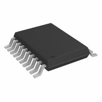
AD7998BRU-1 Analog Devices Inc, AD7998BRU-1 Datasheet - Page 16

AD7998BRU-1
Manufacturer Part Number
AD7998BRU-1
Description
IC,Data Acquisition System,8-CHANNEL,12-BIT,TSSOP,20PIN,PLASTIC
Manufacturer
Analog Devices Inc
Datasheet
1.AD7997BRUZ-1.pdf
(32 pages)
Specifications of AD7998BRU-1
Number Of Bits
12
Sampling Rate (per Second)
188k
Data Interface
I²C, Serial
Number Of Converters
1
Power Dissipation (max)
2.2mW
Voltage Supply Source
Single Supply
Operating Temperature
-40°C ~ 85°C
Mounting Type
Surface Mount
Package / Case
20-TSSOP (0.173", 4.40mm Width)
Lead Free Status / RoHS Status
Contains lead / RoHS non-compliant
For Use With
EVAL-AD7998CBZ - BOARD EVALUATION FOR AD7998CBZ
Lead Free Status / RoHS Status
Contains lead / RoHS non-compliant
AD7997/AD7998
TYPICAL CONNECTION DIAGRAM
The typical connection diagram for the AD7997/AD7998 is
shown in Figure 22. In this figure, the address select pin (AS)
is tied to V
floating, allowing the user to select up to five AD7997/AD7998
devices on the same serial bus. An external reference must be
applied to the AD7997/AD7998. This reference can be in the
range of 1.2 V to V
family, AD780, ADR03, or ADR381 can be used to supply the
reference voltage to the ADC.
SDA and SCL form the 2-wire I
interface. External pull-up resisters are required for both SDA
and SCL lines.
The AD7998-0/AD7997-0 support standard and fast I
interface modes. The AD7998-1/AD7997-1 support standard,
fast, and high speed I
in either standard or fast mode, up to five AD7997/AD7998
devices can be connected to the bus, as noted:
In high speed mode, up to three AD7997-1/AD7998-1 devices
can be connected to the bus.
Wake-up from shutdown and acquisition prior to a conversion
is approximately 1 µs, and conversion time is approximately
2 µs. The AD7997/AD7998 enters shutdown mode again after
each conversion, which is useful in applications where power
consumption is a concern.
3 × AD7997-0/AD7998-0 and 2 × AD7997-1/ AD7998-1
or
3 × AD7997-1/AD7998-1 and 2 × AD7997-0/AD7998-0
DD
; however, AS can also be tied to AGND or left
DD
. A precision reference like the REF 19x
2
C interface modes. Therefore if operating
REF 19x
0.1µF
2
C-/SMBus-compatible
0V to REF
INPUT
1µF
IN
Figure 22. AD7997/AD7998 Typical Connection Diagram
V
V
REF
IN
IN
1
8
IN
2
C
AD7997/
AD7998
AGND
Rev. 0 | Page 16 of 32
V
DD
10µF
CONVST
ALERT
SDA
SCL
AS
0.1µF
ANALOG INPUT
Figure 21 shows an equivalent circuit of the AD7997/AD7998
analog input structure. The two diodes, D1 and D2, provide
ESD protection for the analog inputs. Care must be taken to
ensure that the analog input signal does not exceed the supply
rails by more than 300 mV. This causes the diodes to become
forward biased and start conducting current into the substrate.
These diodes can conduct a maximum current of 10 mA
without causing irreversible damage to the part.
Capacitor C1 in Figure 21 is typically about 4 pF and can
primarily be attributed to pin capacitance. Resistor R1 is a
lumped component made up of the on resistance (R
a track-and-hold switch, and also includes the R
input multiplexer. The total resistance is typically about 400 Ω.
C2, the ADC sampling capacitor, has a typical capacitance of
30 pF.
V
IN
4pF
C1
V
DD
R
P
R
P
Figure 21. Equivalent Analog Input Circuit
R
P
V
DD
5V SUPPLY
D1
D2
2-WIRE SERIAL
INTERFACE
CONVERSION PHASE—SWITCH OPEN
TRACK PHASE—SWITCH CLOSED
µC/µP
R1
30pF
C2
ON
of the
ON
) of


