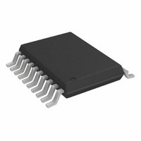
AD7998BRU-1 Analog Devices Inc, AD7998BRU-1 Datasheet - Page 26

AD7998BRU-1
Manufacturer Part Number
AD7998BRU-1
Description
IC,Data Acquisition System,8-CHANNEL,12-BIT,TSSOP,20PIN,PLASTIC
Manufacturer
Analog Devices Inc
Datasheet
1.AD7997BRUZ-1.pdf
(32 pages)
Specifications of AD7998BRU-1
Number Of Bits
12
Sampling Rate (per Second)
188k
Data Interface
I²C, Serial
Number Of Converters
1
Power Dissipation (max)
2.2mW
Voltage Supply Source
Single Supply
Operating Temperature
-40°C ~ 85°C
Mounting Type
Surface Mount
Package / Case
20-TSSOP (0.173", 4.40mm Width)
Lead Free Status / RoHS Status
Contains lead / RoHS non-compliant
For Use With
EVAL-AD7998CBZ - BOARD EVALUATION FOR AD7998CBZ
Lead Free Status / RoHS Status
Contains lead / RoHS non-compliant
AD7997/AD7998
READING DATA FROM THE AD7997/AD7998
Reading data from the AD7997/AD7998 is a 1- or 2-byte
operation. Reading back the contents of the alert status register
or the cycle timer register is a single-byte read operation, as
shown in Figure 29. This assumes the particular register address
has previously been set up by a single-byte write operation to
the address pointer register, as shown in Figure 26. Once the
register address has been set up, any number of reads can be
performed from that particular register without having to write
to the address pointer register again.
If a read from a different register is required, the relevant
register address has to be written to the address pointer register,
and again any number of reads from this register may then be
performed.
SDA
SCL
SDA
SCL
START BY
START BY
MASTER
MASTER
0
1
0
1
1
1
SERIAL BUS ADDRESS BYTE
SERIAL BUS ADDRESS BYTE
0
0
A3
FRAME 1
A3
Figure 30. Reading Two Bytes of Data from the Conversion Result Register
FRAME 1
Figure 29. Reading a Single Byte of Data from a Selected Register
A2
A2
SCL (CONTINUED)
SDA (CONTINUED)
A1
A1
AD7997/AD7998
A0
A0
ACK. BY
R/W
R/W
AD7997/AD7998
Rev. 0 | Page 26 of 32
ACK. BY
9
9
ALERT
FLAG
D7
1
D7
1
1
Reading data from the configuration register, conversion result
register, DATA
registers is a 2-byte operation, as shown in Figure 30. The same
rules apply for a 2-byte read as a single-byte read.
When reading data back from a register, for example the
conversion result register, if more than two read bytes are
supplied, the same or new data is read from the AD7997/
AD7998 without the need to readdress the device. This allows
the master to continuously read from a data register without
having to readdress the AD7997/AD7998.
CHID2
D6
D6
SINGLE DATA BYTE FROM AD7997/AD7998
MOST SIGNIFICANT DATA BYTE FROM
MOST SIGNIFICANT DATA BYTE FROM
CH
D5
D5
ID1
CH
D4
D4
AD7997/AD7998
AD7997/AD7998
ID0
HIGH
FRAME 2
FRAME 2
FRAME 2
D11
D3
D3
registers, DATA
D2
D10
D2
D1
D1/0
D9
D0
D0/0
D8
NO ACK. BY
NO ACK. BY
MASTER
LOW
MASTER
MASTER
ACK. BY
9
9
registers, or hysteresis
9
STOP BY
STOP BY
MASTER
MASTER


