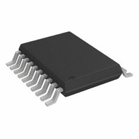
AD7998BRU-1 Analog Devices Inc, AD7998BRU-1 Datasheet - Page 30

AD7998BRU-1
Manufacturer Part Number
AD7998BRU-1
Description
IC,Data Acquisition System,8-CHANNEL,12-BIT,TSSOP,20PIN,PLASTIC
Manufacturer
Analog Devices Inc
Datasheet
1.AD7997BRUZ-1.pdf
(32 pages)
Specifications of AD7998BRU-1
Number Of Bits
12
Sampling Rate (per Second)
188k
Data Interface
I²C, Serial
Number Of Converters
1
Power Dissipation (max)
2.2mW
Voltage Supply Source
Single Supply
Operating Temperature
-40°C ~ 85°C
Mounting Type
Surface Mount
Package / Case
20-TSSOP (0.173", 4.40mm Width)
Lead Free Status / RoHS Status
Contains lead / RoHS non-compliant
For Use With
EVAL-AD7998CBZ - BOARD EVALUATION FOR AD7998CBZ
Lead Free Status / RoHS Status
Contains lead / RoHS non-compliant
AD7997/AD7998
MODE 3—AUTOMATIC CYCLE INTERVAL MODE
An automatic conversion cycle can be selected and enabled by
writing a value to the cycle timer register. A conversion cycle
interval can be set up on the AD7997/AD7998 by programming
the relevant bits in the 8-bit cycle timer register, as decoded in
Table 24. Only the 3 LSBs are used to select the cycle interval;
the 5 MSBs should contain 0s. When the 3 LSBs of the register
are programmed with any configuration other than all 0s, a
conversion takes place every X ms; the cycle interval, X,
depends on the configuration of these three bits in the cycle
timer register. There are seven different cycle time intervals to
choose from, as shown in Table 24. Once the conversion has
taken place, the part powers down again until the next conver-
sion occurs. To exit this mode of operation, the user must
program the 3 LSBs of the cycle timer register to contain all 0s.
SCL
SDA
SDA
SCL
SDA
SDA
SCL
SCL
Sr
S
1
1
7-BIT ADDRESS
7-BIT ADDRESS
Sr
S
1
1
AD7997/AD7998
AD7997/AD7998
W A
8
R A
ACK BY
ACK BY
7-BIT ADDRESS
7-BIT ADDRESS
9
9
1
1
COMMAND/ADDRESS
FIRST DATA BYTE
POINT BYTE
(MSBs)
AD7997/AD7998
AD7997/AD7998
ACK BY
Figure 34. Mode 2 Sequence Operation
W
8
R
AD7997/AD7998
ACK BY
A
A
9
MASTER
9
RESULT FROM CH1
ACK BY
Figure 33. Mode 2 Operation
ACK BY
A
A
1
1
9
9
Rev. 0 | Page 30 of 32
COMMAND/ADDRESS
SECOND DATA BYTE
FIRST DATA BYTE
POINT BYTE
(LSBs)
(MSBs)
A
To select a channel(s) for operation in the cycle mode, set the
corresponding channel bit(s), D11 to D4, of the configuration
register. If more than one channel bit is set in the configuration
register, the ADC automatically cycles through the channel
sequence starting with the lowest channel and working its way
up through the sequence. Once the sequence is complete, the
ADC starts converting on the lowest channel again, continuing
to loop through the sequence until the cycle timer register
contents are set to all 0s. This mode is useful for monitoring
signals, such as battery voltage and temperature, alerting only
when the limits are violated.
MASTER
ACK BY
AD7997/AD7998
A
9
MASTER
ACK BY
ACK BY
9
A
A
9
FIRST DATA BYTE
(MSBs)
SECOND DATA BYTE
(LSBs)
RESULT FROM CH2
MASTER
ACK BY
A
9
SECOND DATA BYTE
NACK BY
MASTER
(LSBs)
A
9
Sr/P
A/A
9


