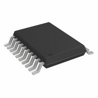
AD7998BRU-1 Analog Devices Inc, AD7998BRU-1 Datasheet - Page 28

AD7998BRU-1
Manufacturer Part Number
AD7998BRU-1
Description
IC,Data Acquisition System,8-CHANNEL,12-BIT,TSSOP,20PIN,PLASTIC
Manufacturer
Analog Devices Inc
Datasheet
1.AD7997BRUZ-1.pdf
(32 pages)
Specifications of AD7998BRU-1
Number Of Bits
12
Sampling Rate (per Second)
188k
Data Interface
I²C, Serial
Number Of Converters
1
Power Dissipation (max)
2.2mW
Voltage Supply Source
Single Supply
Operating Temperature
-40°C ~ 85°C
Mounting Type
Surface Mount
Package / Case
20-TSSOP (0.173", 4.40mm Width)
Lead Free Status / RoHS Status
Contains lead / RoHS non-compliant
For Use With
EVAL-AD7998CBZ - BOARD EVALUATION FOR AD7998CBZ
Lead Free Status / RoHS Status
Contains lead / RoHS non-compliant
AD7997/AD7998
MODES OF OPERATION
When supplies are first applied to the AD7997/AD7998, the
ADC powers up in sleep mode and normally remains in this
shutdown state while not converting. There are three methods
of initiating a conversion on the AD7997/AD7998.
MODE 1—USING THE CONVST PIN
A conversion can be initiated on the AD7997/AD7998 by
pulsing the CONVST signal. The conversion clock for the part
is internally generated so no external clock is required, except
when reading from or writing to the serial port. On the rising
edge of CONVST , the AD7997/AD7998 begins to power up (see
point A in Figure 32). The power-up time from shutdown mode
for the AD7997/AD7998 is approximately 1 µs; the CONVST
signal must remain high for 1 µs for the part to power up fully.
CONVST can be brought low after this time. This power-up
time also includes the acquisition time of the ADC. The falling
edge of the CONVST signal places the track-and-hold into hold
mode; a conversion is also initiated at this point (point B in
Figure 32). When the conversion is complete, approximately
2 µs later, the part returns to shutdown (point C in Figure 32)
and remains there until the next rising edge of CONVST . The
master can then read the ADC to obtain the conversion result.
The address pointer register must be pointing to the conversion
result register in order to read back the conversion result.
CONVST
SCA
SDA
t
A
POWER-UP
B
t
CONVERT
C
S
1
7-BIT ADDRESS
Figure 32. Mode 1 Operation
R
A
Rev. 0 | Page 28 of 32
9
1
FIRST DATA BYTE (MSBs)
If the CONVST pulse does not remain high for more than 1 µs,
the falling edge of CONVST still initiates a conversion but the
result is invalid because the AD7997/AD7998 are not fully
powered-up when the conversion takes place. To maintain the
performance of the AD7997/AD7998 in this mode it is
recommended that the I
taking place.
The cycle timer register and Bits C4 to C1 in the address pointer
register should contain all 0s when operating the AD7997/
AD7998 in this mode. The CONVST pin should be tied low for
all other modes of operation.
To select an analog input channel for conversion in this mode,
the user must write to the configuration register and select the
corresponding channel for conversion. To set up a sequence of
channels to be converted with each CONVST pulse, set the
corresponding channel bits in the configuration register (see
Table 11).
Once a conversion is complete, the master can address the
AD7997/AD7998 to read the conversion result. If further
conversions are required, the SCL line can be taken high while
the CONVST signal is pulsed again; then an additional 18 SCL
pulses are required to read the conversion result.
When operating the AD7997-1/AD7998-1 in Mode 1 and
reading after conversion with a 3.4 MHz f
achieve a typical throughput rate of up to 121 kSPS.
A
9
SECOND DATA BYTE (LSBs)
2
C bus is quiet when a conversion is
SCL
A
9
, the ADCs can
P


