AD9222-65EBZ Analog Devices Inc, AD9222-65EBZ Datasheet - Page 25
AD9222-65EBZ
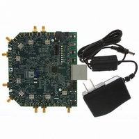
Manufacturer Part Number
AD9222-65EBZ
Description
Octal 12 Bit, 65 MSPS Serial LVDS ADC EB
Manufacturer
Analog Devices Inc
Datasheet
1.AD9222ABCPZRL7-50.pdf
(60 pages)
Specifications of AD9222-65EBZ
Number Of Adc's
8
Number Of Bits
12
Sampling Rate (per Second)
65M
Data Interface
Serial
Inputs Per Adc
2 Single
Input Range
2 Vpp
Power (typ) @ Conditions
910mW @ 65MSPS
Voltage Supply Source
Single Supply
Operating Temperature
-40°C ~ 85°C
Utilized Ic / Part
AD9222
Kit Application Type
Data Converter
Application Sub Type
ADC
Features
Serial LVDS, Data And Frame Clock Outputs, 325MHz Full-power Analog Bandwidth
Lead Free Status / RoHS Status
Lead free / RoHS Compliant
Lead Free Status / RoHS Status
Lead free / RoHS Compliant


Clock Jitter Considerations
High speed, high resolution ADCs are sensitive to the quality of the
clock input. The degradation in SNR at a given input frequency
(f
In this equation, the rms aperture jitter represents the root mean
square of all jitter sources, including the clock input, analog input
signal, and ADC aperture jitter specifications. IF undersampling
applications are particularly sensitive to jitter (see Figure 68).
The clock input should be treated as an analog signal in cases
where aperture jitter may affect the dynamic range of the AD9222.
Power supplies for clock drivers should be separated from the
ADC output driver supplies to avoid modulating the clock signal
with digital noise. Low jitter, crystal-controlled oscillators make
the best clock sources. If the clock is generated from another
type of source (by gating, dividing, or other methods), it should
be retimed by the original clock at the last step.
Refer to the AN-501 Application Note and the AN-756
Application Note for more in-depth information about jitter
performance as it relates to ADCs.
A
) due only to aperture jitter (t
SNR Degradation = 20 × log 10(1/2 × π × f
130
120
100
110
90
80
70
60
50
40
30
1
10 BITS
8 BITS
RMS CLOCK JITTER REQUIREMENT
Figure 68. Ideal SNR vs. Input Frequency and Jitter
ANALOG INPUT FREQUENCY (MHz)
10
0.125ps
0.25ps
J
0.5ps
1.0ps
2.0ps
) can be calculated by
100
A
× t
16 BITS
14 BITS
12 BITS
J
)
1000
Rev. D | Page 25 of 60
Power Dissipation and Power-Down Mode
As shown in Figure 69, the power dissipated by the AD9222 is
proportional to its sample rate. The digital power dissipation
does not vary much because it is determined primarily by the
DRVDD supply and bias current of the LVDS output drivers.
500
450
400
350
300
250
200
150
100
0.40
0.35
0.30
0.25
0.20
0.15
0.10
0.05
50
Figure 69. Supply Current vs. f
0
Figure 70. Supply Current vs. f
0
10
10
AVDD CURRENT
15
AVDD CURRENT
20
DRVDD CURRENT
20
30
ENCODE (MSPS)
25
ENCODE (MSPS)
DRVDD CURRENT
TOTAL POWER
SAMPLE
SAMPLE
30
40
for f
for f
TOTAL POWER
35
IN
IN
= 10.3 MHz, AD9222- 50
= 10.3 MHz, AD9222- 65
50
40
45
60
AD9222
50
950
900
850
800
750
700
0.800
0.750
0.700
0.650
0.600
0.550
0.500
Related parts for AD9222-65EBZ
Image
Part Number
Description
Manufacturer
Datasheet
Request
R

Part Number:
Description:
Octal 12 Bit, 50 MSPS Serial LVDS ADC EB
Manufacturer:
Analog Devices Inc
Datasheet:

Part Number:
Description:
±1.7g Dual-Axis IMEMS Accelerometer Evaluation Board
Manufacturer:
Analog Devices Inc
Datasheet:
Part Number:
Description:
Inertial Sensor Evaluation System
Manufacturer:
Analog Devices Inc
Datasheet:
Part Number:
Description:
Manufacturer:
Analog Devices Inc
Datasheet:
Part Number:
Description:
Manufacturer:
Analog Devices Inc
Datasheet:
Part Number:
Description:
Manufacturer:
Analog Devices Inc
Datasheet:
Part Number:
Description:
Manufacturer:
Analog Devices Inc
Datasheet:
Part Number:
Description:
Manufacturer:
Analog Devices Inc
Datasheet:
Part Number:
Description:
Manufacturer:
Analog Devices Inc
Datasheet:
Part Number:
Description:
Manufacturer:
Analog Devices Inc
Datasheet:
Part Number:
Description:
Manufacturer:
Analog Devices Inc
Datasheet:
Part Number:
Description:
Manufacturer:
Analog Devices Inc
Datasheet:
Part Number:
Description:
Manufacturer:
Analog Devices Inc
Datasheet: