AD9222-65EBZ Analog Devices Inc, AD9222-65EBZ Datasheet - Page 26
AD9222-65EBZ
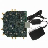
Manufacturer Part Number
AD9222-65EBZ
Description
Octal 12 Bit, 65 MSPS Serial LVDS ADC EB
Manufacturer
Analog Devices Inc
Datasheet
1.AD9222ABCPZRL7-50.pdf
(60 pages)
Specifications of AD9222-65EBZ
Number Of Adc's
8
Number Of Bits
12
Sampling Rate (per Second)
65M
Data Interface
Serial
Inputs Per Adc
2 Single
Input Range
2 Vpp
Power (typ) @ Conditions
910mW @ 65MSPS
Voltage Supply Source
Single Supply
Operating Temperature
-40°C ~ 85°C
Utilized Ic / Part
AD9222
Kit Application Type
Data Converter
Application Sub Type
ADC
Features
Serial LVDS, Data And Frame Clock Outputs, 325MHz Full-power Analog Bandwidth
Lead Free Status / RoHS Status
Lead free / RoHS Compliant
Lead Free Status / RoHS Status
Lead free / RoHS Compliant


AD9222
By asserting the PDWN pin high, the AD9222 is placed into
power-down mode. In this state, the ADC typically dissipates
11 mW. During power-down, the LVDS output drivers are placed
in a high impedance state. The AD9222 returns to normal
operating mode when the PDWN pin is pulled low. This pin is
both 1.8 V and 3.3 V tolerant.
In power-down mode, low power dissipation is achieved by
shutting down the reference, reference buffer, PLL, and biasing
networks. The decoupling capacitors on REFT and REFB are
discharged when entering power-down mode and must be
recharged when returning to normal operation. As a result, the
wake-up time is related to the time spent in the power-down
mode; shorter cycles result in proportionally shorter wake-up
times. With the recommended 0.1 μF and 4.7 μF decoupling
capacitors on REFT and REFB, approximately 1 sec is required
to fully discharge the reference buffer decoupling capacitors,
and approximately 375 μs is required to restore full operation.
There are several other power-down options available when
using the SPI. The user can individually power down each
channel or put the entire device into standby mode. The latter
option allows the user to keep the internal PLL powered when
fast wake-up times (~600 ns) are required. See the Memory
Map section for more details on using these features.
Digital Outputs and Timing
The AD9222 differential outputs conform to the ANSI-644 LVDS
standard on default power-up. This can be changed to a low power,
reduced signal option (similar to the IEEE 1596.3 standard) via the
SDIO/ODM pin or SPI. This LVDS standard can further reduce
the overall power dissipation of the device by approximately
36 mW. See the SDIO/ODM Pin section or Table 16 in the
Memory Map section for more information. The LVDS driver
current is derived on chip and sets the output current at each
output equal to a nominal 3.5 mA. A 100 Ω differential termination
resistor placed at the LVDS receiver inputs results in a nominal
350 mV swing at the receiver.
The AD9222 LVDS outputs facilitate interfacing with LVDS
receivers in custom ASICs and FPGAs for superior switching
performance in noisy environments. Single point-to-point net
topologies are recommended with a 100 Ω termination resistor
Rev. D | Page 26 of 60
placed as close to the receiver as possible. If there is no far-end
receiver termination or there is poor differential trace routing,
timing errors may result. To avoid such timing errors, it is
recommended that the trace length be no longer than 24 inches
and that the differential output traces be kept close together and
at equal lengths. An example of the FCO and data stream with
proper trace length and position is shown in Figure 71.
Figure 71. LVDS Output Timing Example in ANSI-644 Mode (Default),
Figure 72. LVDS Output Timing Example in ANSI-644 Mode (Default),
CH1 500mV/DIV = FCO
CH2 500mV/DIV = DCO
CH3 500mV/DIV = DATA
CH1 500mV/DIV = FCO
CH2 500mV/DIV = DCO
CH3 500mV/DIV = DATA
AD9222-50
AD9222-65
5.0ns/DIV
5.0ns/DIV
Related parts for AD9222-65EBZ
Image
Part Number
Description
Manufacturer
Datasheet
Request
R

Part Number:
Description:
Octal 12 Bit, 50 MSPS Serial LVDS ADC EB
Manufacturer:
Analog Devices Inc
Datasheet:

Part Number:
Description:
±1.7g Dual-Axis IMEMS Accelerometer Evaluation Board
Manufacturer:
Analog Devices Inc
Datasheet:
Part Number:
Description:
Inertial Sensor Evaluation System
Manufacturer:
Analog Devices Inc
Datasheet:
Part Number:
Description:
Manufacturer:
Analog Devices Inc
Datasheet:
Part Number:
Description:
Manufacturer:
Analog Devices Inc
Datasheet:
Part Number:
Description:
Manufacturer:
Analog Devices Inc
Datasheet:
Part Number:
Description:
Manufacturer:
Analog Devices Inc
Datasheet:
Part Number:
Description:
Manufacturer:
Analog Devices Inc
Datasheet:
Part Number:
Description:
Manufacturer:
Analog Devices Inc
Datasheet:
Part Number:
Description:
Manufacturer:
Analog Devices Inc
Datasheet:
Part Number:
Description:
Manufacturer:
Analog Devices Inc
Datasheet:
Part Number:
Description:
Manufacturer:
Analog Devices Inc
Datasheet:
Part Number:
Description:
Manufacturer:
Analog Devices Inc
Datasheet: