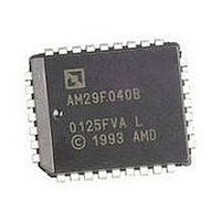
AM29F002BT-90JC Spansion Inc., AM29F002BT-90JC Datasheet - Page 11

AM29F002BT-90JC
Manufacturer Part Number
AM29F002BT-90JC
Description
Flash Memory IC
Manufacturer
Spansion Inc.
Datasheet
1.AM29F002BT-90JC.pdf
(42 pages)
Specifications of AM29F002BT-90JC
Memory Size
2Mbit
Memory Configuration
256K X 8
Ic Interface Type
Parallel
Access Time
90ns
Memory Case Style
PLCC
No. Of Pins
32
Operating Temperature Range
0°C To +70°C
Termination Type
SMD
Available stocks
Company
Part Number
Manufacturer
Quantity
Price
Company:
Part Number:
AM29F002BT-90JC
Manufacturer:
ROHM
Quantity:
6 221
Status” for more information, and to each AC Charac-
teristics section for timing diagrams.
Standby Mode
When the system is not reading or writing to the device,
it can place the device in the standby mode. In this
mode, current consumption is greatly reduced, and the
outputs are placed in the high impedance state, inde-
pendent of the OE# input.
The device enters the CMOS standby mode when CE#
and RESET# pins (CE# only on the Am29F002NB) are
both held at V
restricted voltage range than V
the TTL standby mode when CE# and RESET# pins
(CE# only on the Am29F002NB) are both held at V
The device requires standard access time (t
access when the device is in either of these standby
modes, before it is ready to read data.
The device also enters the standby mode when the
RESET# pin is driven low. Refer to the next section,
“RESET#: Hardware Reset Pin”.
If the device is deselected during erasure or program-
ming, the device draws active current until the
operation is completed.
In the DC Characteristics tables, I
standby current specification.
November 1, 2006 21527D5
Sector
SA0
SA1
SA2
SA3
SA4
SA5
SA6
CC
A17
Table 2. Am29F002B/Am29F002NB Top Boot Block Sector Address Table
0
0
1
1
1
1
1
± 0.5 V. (Note that this is a more
A16
0
1
0
1
1
1
1
IH
.) The device enters
CC3
A15
X
X
X
0
1
1
1
represents the
Am29F002B/Am29F002NB
CE
D A T A
) for read
A14
X
X
X
X
0
0
1
IH
.
S H E E T
A13
X
X
X
X
X
0
1
RESET#: Hardware Reset Pin
Note: The RESET# pin is not available on the
Am29F002NB.
The RESET# pin provides a hardware method of reset-
ting the device to reading array data. When the system
drives the RESET# pin low for at least a period of t
the device immediately terminates any operation in
progress, tristates all data output pins, and ignores all
read/write attempts for the duration of the RESET#
pulse. The device also resets the internal state
machine to reading array data. The operation that was
interrupted should be reinitiated once the device is
ready to accept another command sequence, to
ensure data integrity.
Current is reduced for the duration of the RESET#
pulse. When RESET# is held at V
the TTL standby mode; if RESET# is held at V
0.5 V, the device enters the CMOS standby mode.
The RESET# pin may be tied to the system reset cir-
cuitry. A system reset would thus also reset the Flash
memory, enabling the system to read the boot-up firm-
ware from the Flash memory.
Refer to the AC Characteristics tables for RESET#
parameters and timing diagram.
Output Disable Mode
When the OE# input is at V
disabled. The output pins are placed in the high imped-
ance state.
Sector Size
(Kbytes)
64
64
64
32
16
8
8
IH
, output from the device is
(in hexadecimal)
3A000h–3BFFFh
3C000h–3FFFFh
00000h–0FFFFh
10000h–1FFFFh
20000h–2FFFFh
30000h–37FFFh
38000h–39FFFh
Address Range
IL
, the device enters
SS
RP
9
±
,


