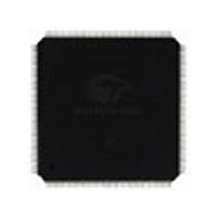
CY7C09579V-83AXC Cypress Semiconductor Corp, CY7C09579V-83AXC Datasheet - Page 24

CY7C09579V-83AXC
Manufacturer Part Number
CY7C09579V-83AXC
Description
IC,SYNC SRAM,32KX36,CMOS,QFP,144PIN,PLASTIC
Manufacturer
Cypress Semiconductor Corp
Specifications of CY7C09579V-83AXC
Format - Memory
RAM
Memory Type
SRAM - Dual Port, Synchronous
Memory Size
1.152M (32K x 36)
Speed
83MHz
Interface
Parallel
Voltage - Supply
3 V ~ 3.6 V
Operating Temperature
0°C ~ 70°C
Package / Case
144-LQFP
Density
1.125Mb
Access Time (max)
18ns
Sync/async
Synchronous
Architecture
SDR
Clock Freq (max)
45MHz
Operating Supply Voltage (typ)
3.3V
Address Bus
15b
Package Type
TQFP
Operating Temp Range
0C to 70C
Number Of Ports
2
Supply Current
360mA
Operating Supply Voltage (min)
3.135V
Operating Supply Voltage (max)
3.465V
Operating Temperature Classification
Commercial
Mounting
Surface Mount
Pin Count
144
Word Size
36b
Number Of Words
32K
Lead Free Status / RoHS Status
Lead free / RoHS compliant by exemption
Lead Free Status / RoHS Status
Lead free / RoHS compliant by exemption
Available stocks
Company
Part Number
Manufacturer
Quantity
Price
Company:
Part Number:
CY7C09579V-83AXC
Manufacturer:
Cypress Semiconductor Corp
Quantity:
10 000
Right Port Configuration
Right Port Operation
Readout of Internal Address Counter
Left Port Operation
Document Number: 38-06054 Rev. *E
Notes
78. BM, SIZE, and BE must be reconfigured 1 cycle before operation is guaranteed. BM, SIZE, and BE should remain static for any particular port configuration.
79. In x36 mode, BE input is a “Don’t Care.”
80. DQ represents data output of the chip.
81. x18 and x9 configuration apply to right port only.
Configuration
Configuration
Right Port x36
Right Port x18
Right Port x9
Left Port x36
x18
x18
x9
x9
BM
0
1
1
Control Pin
Address on 1st Cycle
B0
B1
B2
B3
BE
0
1
0
1
WA, A
[80]
A
A
A
0R–14R
6R–14R
0L–14L
0R–14R
[78, 79]
SIZE
Data on 1st Cycle
0
0
1
DQ
DQ
DQ
DQ
18R–35R
27R–35R
0R–17R
0R–8R
I/O Pins used on 1st Cycle
[81]
I/O
I/O
I/O
I/O
Data on 2nd Cycle
Configuration
3R–17R
2R–17R
3L–17L
0R–8R
DQ
DQ
DQ
DQ
18R–35R
18R–26R
x36
x18
0R–17R
9R–17R
x9
I/O
I/O
I/O
I/O
Address on 2nd
18–26
27–35
BA, WA, A
9–17
0–8
Data on 3rd Cycle
Effect
Byte Control
Byte Control
Cycle
Byte Control
Byte Control
DQ
DQ
–
–
–
18R–26R
9R–17R
–
–
0R–5R
I/O Pins used
I/O
I/O
I/O Pins used on 2nd
I/O
0R–35R
0R–17R
0R–8R
Data on 4th Cycle
I/O
CY7C09569V
CY7C09579V
DQ
Cycle
DQ
1R–8R
–
–
–
27R–35R
0R–8R
–
–
Page 24 of 32
[+] Feedback


