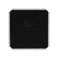
CY7C09579V-83AXC Cypress Semiconductor Corp, CY7C09579V-83AXC Datasheet - Page 6

CY7C09579V-83AXC
Manufacturer Part Number
CY7C09579V-83AXC
Description
IC,SYNC SRAM,32KX36,CMOS,QFP,144PIN,PLASTIC
Manufacturer
Cypress Semiconductor Corp
Specifications of CY7C09579V-83AXC
Format - Memory
RAM
Memory Type
SRAM - Dual Port, Synchronous
Memory Size
1.152M (32K x 36)
Speed
83MHz
Interface
Parallel
Voltage - Supply
3 V ~ 3.6 V
Operating Temperature
0°C ~ 70°C
Package / Case
144-LQFP
Density
1.125Mb
Access Time (max)
18ns
Sync/async
Synchronous
Architecture
SDR
Clock Freq (max)
45MHz
Operating Supply Voltage (typ)
3.3V
Address Bus
15b
Package Type
TQFP
Operating Temp Range
0C to 70C
Number Of Ports
2
Supply Current
360mA
Operating Supply Voltage (min)
3.135V
Operating Supply Voltage (max)
3.465V
Operating Temperature Classification
Commercial
Mounting
Surface Mount
Pin Count
144
Word Size
36b
Number Of Words
32K
Lead Free Status / RoHS Status
Lead free / RoHS compliant by exemption
Lead Free Status / RoHS Status
Lead free / RoHS compliant by exemption
Available stocks
Company
Part Number
Manufacturer
Quantity
Price
Company:
Part Number:
CY7C09579V-83AXC
Manufacturer:
Cypress Semiconductor Corp
Quantity:
10 000
Pin Definitions
Document Number: 38-06054 Rev. *E
A
ADS
CE
CLK
CNTEN
CNTRST
I/O
OE
R/W
FT/PIPE
B
–
–
V
V
0L
0L
SS
DD
Left Port
0L
L
L
–A
–B
L
L
L
–I/O
13/14L
3L
L
L
L
35L
A
ADS
CE
CLK
CNTEN
CNTRST
I/O
OE
R/W
FT/PIPE
–
BM, SIZE
BE
0R
Right Port
0R
R
R
–A
R
R
R
–I/O
13/14R
R
R
R
35R
Address Inputs (A
Address Strobe Input. Used as an address qualifier. This signal should be asserted LOW to assert
the part using the externally supplied address on Address Pins. To load this address into the Burst
Address Counter both ADS and CNTEN have to be LOW. ADS is disabled if CNTRST is asserted
LOW
Chip Enable Input
Clock Signal. This input can be free-running or strobed. Maximum clock input rate is f
Counter Enable Input. Asserting this signal LOW increments the burst address counter of its
respective port on each rising edge of CLK. CNTEN is disabled if CNTRST is asserted LOW
Counter Reset Input. Asserting this signal LOW resets the burst address counter of its respective
port to zero. CNTRST is not disabled by asserting ADS or CNTEN
Data Bus Input/Output
Output Enable Input. This signal must be asserted LOW to enable the I/O data pins during read
operations
Read/Write Enable Input. This signal is asserted LOW to write to the dual port memory array. For
read operations, assert this pin HIGH
Flow-Through/Pipelined Select Input. For flow-through mode operation, assert this pin LOW. For
pipelined mode operation, assert this pin HIGH
Byte Select Inputs. Asserting these signals enable read and write operations to the corresponding
bytes of the memory array
Select Pins for Bus Matching. See Bus Matching for details
Big Endian Pin. See Bus Matching for details
Ground Input
Power Input
0
–A
13
for 16 K, A
0
–A
14
for 32 K devices)
Description
CY7C09569V
CY7C09579V
Page 6 of 32
MAX
[+] Feedback


